Introduction
A 555 Timer IC is a multipurpose circuit chip that is used in timer, pulse generation circuits and oscillation circuits. It is one of the distinguished and trending inventions of today’s technological world. The 555 timer integrated circuit (IC) was first designed by Hans Camenzind, a Swiss electronics engineer. Camenzind worked for several months on the final design to build different test iterations by hand on a breadboard with discrete components. A 555 timer IC is a multipurpose integrated circuit chip that finds its application in timer, oscillation and pulse generation circuits. It is one of the prominent and popular inventions of the electronic world. A monolithic timing circuit, the 555 timer, equally reliable and cheap, like op-amps working in the same areas. It can produce
When the design was finalized, Camenzind sat at a drafting table and used a razor to cut the circuit design into a sheet of plastic. In total 23 BJTs, 15 resistors, and 2 diodes were cut into the plastic. This was then reduced to produce the etching mask for etching onto the silicon wafers. That kind of beginning-to-end design work by one man is now done by large teams of engineers with complex design, simulation, routing, and etching software to handle the difficult task of modern IC design.
555 Timer IC Fundamentals
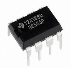
The 555 Timer is a digital monolithic integrated circuit that serves as a highly versatile clock generator in electronic systems. This integrated circuit can be configured as either a stable or monostable multivibrator, making it adaptable to countless timing applications. Developed in 1970 by Signetics Corporation and designed by Hans Camenzind in 1971, the 555 timer IC operates as a linear device with excellent compatibility with both CMOS and TTL digital circuits. The standard 555 timer integrated circuit comprises 25 transistors, 15 resistors, and 2 diodes, all packaged within a compact 8-pin dual in-line package, making it ideal for space-constrained PCB layouts.
Architecture and Pinout
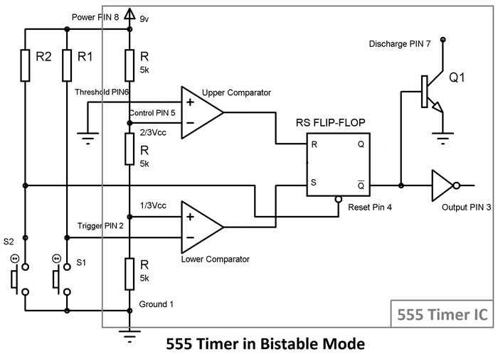
The internal architecture of the 555 timer IC consists of three 5-kilohm resistors connected in series, forming a voltage divider network that gives the IC its famous name. These resistors create reference voltages at one-third and two-thirds of the supply voltage, which are critical for comparator operations. The IC contains two comparators that work together with an internal flip-flop to control the output state, while the internal discharge transistor provides a controlled path for timing capacitor discharge.
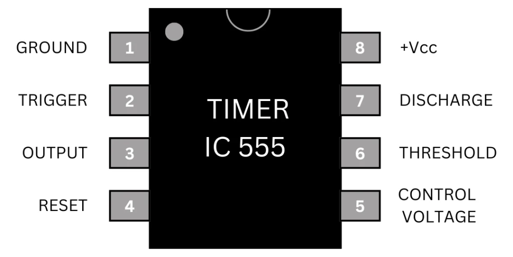
Pinout Description Table
| 1 | Ground (GND) | Connects to circuit ground and serves as the voltage reference point. Proper PCB grounding is critical for stable operation. |
| 2 | Trigger | Starts the timing cycle when voltage drops below one-third of Vcc. Keep traces noise-free through careful PCB routing. |
| 3 | Output | Provides timer output signal, sourcing or sinking up to 200mA. It can directly drive LEDs, relays, or moderate-current loads. |
| 4 | Reset | Active-low input that resets the timer when pulled below 0.7V. Connect to Vcc through pull-up resistor for normal operation. |
| 5 | Control Voltage | Provides access to internal voltage divider at two-thirds Vcc. Bypass to ground with 0.01µF capacitor to prevent noise. |
| 6 | Threshold | Ends timing cycle when voltage exceeds two-thirds of Vcc. Timing capacitor connects here in most configurations. |
| 7 | Discharge | Connects to internal discharge transistor collector. Provides controlled discharge path for timing capacitor. |
| 8 | Vcc | Positive supply voltage (4.5V–16V). Place 0.1µF ceramic decoupling capacitor close to this pin on PCB. |
PCB Package Options
The 555 timer IC is available in 8-pin DIP for through-hole mounting and 8-pin SOIC for surface-mount applications. DIP packages feature 0.3-inch row spacing with holes sized 0.8-1.0mm diameter. Surface-mount variants require precise pad dimensions for proper solder fillet formation. Always include orientation markings and pin-1 indicators on the PCB to prevent assembly errors.
Operating Modes
The 555 timer integrated circuit operates in three distinct modes, each serving different timing and oscillation needs in PCB applications. The IC works across a wide voltage range from 4.5V to 15V DC, making it suitable for various power supply configurations.
Monostable Mode
In monostable configuration, the 555 timer IC produces a single output pulse when triggered. The timing period is determined by external resistor and capacitor values using the formula T = 1.1 × R × C. For reliable PCB operation, position timing components close to the IC with short traces to minimize noise susceptibility. Include a 0.01µF bypass capacitor on the control voltage pin for stable reference voltage. This mode is ideal for pulse generation, time delay circuits, and touch-activated switches.
Astable Mode
Astable mode generates continuous square wave output without external triggering, perfect for clock generation and oscillator applications. The frequency depends on two resistors and one capacitor, calculated as f = 1.44 / ((R1 + 2×R2) × C). Use stable capacitor types like polyester or ceramic for consistent frequency. Place timing components close together on the PCB to minimize stray capacitance effects. Ensure adequate trace width on the output pin and include series resistors when driving LEDs directly. Ground connections should converge at a single point near the IC to prevent timing jitter.
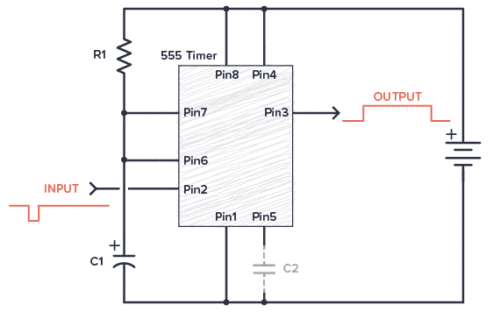
Bistable Mode
Bistable mode creates a flip-flop circuit with two stable states, responding to trigger and reset inputs. The output remains in its last commanded state indefinitely without timing components. This mode is useful for latching circuits, touch switches, and simple memory elements. When implementing on PCBs, include de-bouncing circuits for mechanical switch inputs and pull-up resistors for defined logic levels.
Variants and Alternatives
The CMOS versions like LMC555 and TLC555 offer significant advantages over standard bipolar 555 timers, consuming microamperes instead of milli amperes and operating from lower voltages down to 1.5V. These variants are ideal for battery-powered PCB designs with minimized heat generation. The 556 dual timer IC packages two complete 555 circuits in a 14-pin package, saving board space for designs that need multiple timing functions. Modern microcontrollers can replicate 555 functionalities with added programmability, though the 555 timer IC remains more cost-effective for simple timing applications.
Comparison Table: 555 Timer IC Variants
| Feature | Standard 555 | CMOS 555 | 556 Dual |
| Supply Voltage | 4.5V – 16V | 1.5V – 15V | 4.5V – 16V |
| Supply Current | 3–6 mA | 100–250 µA | 6–12 mA |
| Max Frequency | 500 kHz | 3 MHz | 500 kHz |
| Output Current | 200 mA | 100 mA | 200 mA each |
| Best For | General timing | Battery-powered | Dual channels |
PCB Design Best Practices
Successful 555 timer IC implementation requires careful PCB layout. Position the IC centrally with timing components within 1-2 cm of relevant pins. Place the 0.1µF decoupling capacitor immediately adjacent to the power pin with short, wide traces. Route trigger input traces away from output and discharge pins to prevent false triggering. Use ground plane fills for low impedance return paths and electromagnetic shielding. Ensure adequate copper weight for output current handling and include thermal relief for hand soldering. Select FR-4 material for most applications, with proper trace routing maintaining signal integrity and noise immunity.
Troubleshooting and Testing
Common 555 timer IC issues include timing instability from noisy power supplies or inadequate decoupling. Always place a 0.1µF ceramic capacitor close to the power pin and add a 0.01µF capacitor on the control voltage pin. Component tolerance affects accuracy significantly, so use 1% resistors and high-quality film capacitors for precision timing. Test circuits by verifying supply voltage at pin 8, checking ground connection at pin 1, and using an oscilloscope to observe output waveforms. Monitor threshold and trigger pin voltages during operation to verify proper comparator action.
Practical Applications
The 555 timer IC excels in precision timing circuits for industrial applications using temperature-compensated components. Power management designs leverage PWM capability for switching power supplies and motor speed controllers. Audio applications include tone generators, sirens, and voltage-controlled oscillators for musical effects. The IC’s robust output stage can directly drive power MOSFETs without additional buffering. Applications range from simple LED flashers to sophisticated control systems, demonstrating the continued relevance of this classic integrated circuit in modern PCB designs.
Conclusion
The 555 timer IC remains an important component in PCB design more than fifty years after its invention. Its flexibility extents monostable pulse generation, astable oscillation, and bistable flip-flop operations with reduced external components. Understanding proper Printed circuit board layout techniques, component selection, and operating modes help designers to create reliable and functional timing circuits. CMOS variants and dual-timer packages enhance design possibilities while maintaining compatibility with the original architecture.
At Wonderful PCB, we specialize in manufacturing high-quality circuit boards optimized for 555 timer IC applications. Our experienced team ensures proper component placement, trace routing, and thermal management for reliable performance. Whether you need prototype boards or full production runs, our advanced fabrication capabilities deliver precision Printed circuit boards (PCBs) that meet your specifications. Contact Wonderful PCB today to discuss your project requirements and bring your 555 timer IC designs to life with professional quality and reliability.
Frequently Asked Questions
Can the 555 timer be used in high-frequency applications?
Standard bipolar 555 timers works reliably up to 500 kHz, while CMOS variants like LMC555 reach 3 MHz. Beyond these frequencies, consider specific oscillator ICs. PCB layout with short traces and proper grounding becomes critical at higher frequencies.
What are the PCB layout requirements for precision timing?
Use 1% tolerance resistors and temperature-stable capacitors positioned within 1-2 cm of IC pins. Include 0.1µF decoupling at power pin and 0.01µF at control voltage pin. Implement ground plane or star grounding to minimize interference.
Can 555 timers drive high-current loads directly?
The output can source or sink 200 mA, sufficient for LEDs and small relays. For higher currents or inductive loads, use external driver transistors with flyback diodes for protection.
How do I protect 555 timer circuits from ESD on PCBs?
Add series resistors (10-100 kΩ) on input pins and TVS diodes on external connections. Use ground planes for shielding and ensure proper enclosure grounding for commercial products.
What are thermal considerations for 555 timer PCB layouts?
Standard bipolar 555s generate heat from quiescent current. CMOS variants significantly reduce power consumption. For high-power applications, use larger copper pads, thermal vias, and adequate spacing from heat-sensitive components.