Blog

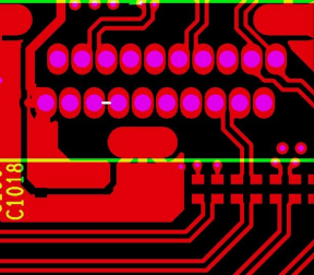
electrical-related safety distances

8 Safety Distances That Must Be Considered in PCB Design

There are many safety distance considerations in PCB design, including spacing between traces, character spacing, pad spacing, and more. Here, we classify them into two categories: electrical-related safety distances and non-electrical-related safety distances. 01 Electrical-Related Safety Distances Trace-to-Trace Spacing For the processing capabilities of mainstream PCB manufacturers, the minimum distance between traces should not be […]

8 Safety Distances That Must Be Considered in PCB Design Read More »

PCB hole spacing

Reliability Analysis of Hole Spacing in PCB Design

The production of single-sided or double-sided PCBs typically involves drilling non-conductive or conductive holes directly after the material is cut, while multi-layer boards are drilled after the lamination process. Holes are categorized based on their function, including component holes, tool holes, through holes (Vias), blind holes, and buried holes (blind and buried holes are a

Reliability Analysis of Hole Spacing in PCB Design Read More »

PCB Manufacturability

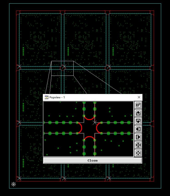
PCB Manufacturability Design and Case Analysis: Silkscreen, Outline, and Panelization

PCB design is a complex process that involves various unforeseen factors that can impact the overall outcome. To ensure high-quality PCB production on time—without extending design time or incurring costly rework—design and circuit integrity issues must be identified early in the process. However, there are many minor details in PCB design that, if overlooked, can

PCB Manufacturability Design and Case Analysis: Silkscreen, Outline, and Panelization Read More »

PCB Manufacturability Holes and Slots

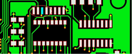
PCB Manufacturability Design and Case Analysis: Holes and Slots

Vias are an unavoidable aspect of PCB design. During the layout process, avoiding all crossover lines is often challenging. To resolve this, vias are used to achieve interlayer connectivity, leading to the development of double-sided and multilayer PCBs. Consequently, vias have become a critical element of PCB design. From a design perspective, vias serve two

PCB Manufacturability Design and Case Analysis: Holes and Slots Read More »

PCB Inner Layer

Manufacturability Design for PCB Inner Layers

When a PCB engineer lays out a product, it involves more than just component placement and routing. Designing the power and ground planes in the inner layers is equally critical. Managing inner layers requires consideration of power integrity, signal integrity, electromagnetic compatibility, and Design for Manufacturability. Difference Between Inner Layers and Outer Layers Outer layers

Manufacturability Design for PCB Inner Layers Read More »

Importance of PCB Layout about Electronic Components in PCBA

Proper installation of electronic components on the PCB is crucial to reducing soldering defects. When arranging electronic components, avoid areas with high deflection values and high internal stress. Distribute components evenly, especially those with high thermal conductivity. Avoid using oversized PCBs to prevent expansion and contraction. Poor PCB layout design can affect the PCB’s manufacturability and

Importance of PCB Layout about Electronic Components in PCBA Read More »

Interconnect Point for Gold Finger

Entire Process of Gold Finger PCB in Design and Manufacturing

In computer memory modules and graphics cards, there is a row of golden conductive contact pads, commonly known as “gold fingers.” In the PCB design and manufacturing industry, the PCB gold finger (Gold Finger or Edge Connector) refers to the connector used as the external interface for the PCB to connect to external devices. In

Entire Process of Gold Finger PCB in Design and Manufacturing Read More »

PCBA

Assisting BOM Error Checking to Support Component Procurement

The Bill of Materials (BOM) for electronic products is a straightforward yet intricate task. With numerous components, even a minor oversight can lead to procuring the wrong components. Manual matching increases the risk of errors. If mistakes occur during the BOM matching stage, subsequent procurement inquiries and customer quotes are likely to be flawed as

Assisting BOM Error Checking to Support Component Procurement Read More »

PCB Design Safety Distances

8 Safety Distances to Consider in PCB Design

PCB design requires attention to numerous safety distances, including trace spacing, text spacing, and pad spacing. These considerations can generally be categorized into two types: electrical safety distances and non-electrical safety distances. 01 Electrical Safety Distances Trace-to-Trace Spacing For mainstream PCB manufacturers, the minimum spacing between traces must not be less than 0.075mm. The minimum

8 Safety Distances to Consider in PCB Design Read More »

How to avoid pitfalls in square slots and square holes of device pins

Introduction Nowadays, circuit boards use more SMD components than plug-in components, but for those electronic products with higher heat dissipation requirements, the performance of plug-in components will be better than that of SMD components. In addition, the external interface of the motherboard and the devices of the connector all use plug-in pins, such as USB,

How to avoid pitfalls in square slots and square holes of device pins Read More »

Easy to use! No need to worry about PCB graphic alignment

Many friends will encounter the situation of graphic misalignment when using wonderfulpcb DFM Services software to import Gerber files. The reason for the misalignment of graphics is that there are unknown objects outside the design file frame, and the canvas size of each layer is different, which causes the coordinates to change with the canvas size

Easy to use! No need to worry about PCB graphic alignment Read More »

Allegro Design File Short Circuit 51

PCB Design Pitfall Avoidance Guide

Ensuring the reliability of electronic product designs is crucial. Manufacturability design encompasses three key aspects: PCB manufacturability design, PCBA assembly design, and cost-effective manufacturing design. Among these, PCB manufacturability design focuses on the manufacturing perspective of PCB boards, considering process parameters to improve production yield and reduce communication costs. Design considerations include line width and

PCB Design Pitfall Avoidance Guide Read More »

The Role of wonderfulpcb DFM Services in Hardware Design and Manufacturing

The PCBA hardware design and manufacturing process involves many links. General hardware products are composed of several stages: hardware design, which includes PCB drawing, PCB circuit board manufacturing, component procurement and inspection, SMT patch processing, plug-in processing, program burning, testing, ageing, and other processes. Let us explain the role of DFM in these links. 1.

The Role of wonderfulpcb DFM Services in Hardware Design and Manufacturing Read More »

PCB bare board analysis 45

Wonderfulpcb DFM Services with DFA is now available!

During the process of PCBA manufacturing and assembly, hardware engineers may often encounter such problems: the PCB design is indeed problematic, the purchased components do not match the actual ones during PBCA processing, the product production cycle is long, and the quality cannot be guaranteed…So how can we discover and solve these manufacturing risks before

Wonderfulpcb DFM Services with DFA is now available! Read More »

wonderfulpcb DFM Visual BOM Interactive Welding Tool is a blessing for SMT factories and PCB engineers!

At present, electronic products have penetrated into every corner of our lives, and their products cover communications, medical, computer peripheral audio-visual products, toys, household appliances, military products, etc. Regarding the PCBA welding of electronic products, manual welding is generally used in the sample stage. The advantage of manual welding is that it is low-cost and

wonderfulpcb DFM Visual BOM Interactive Welding Tool is a blessing for SMT factories and PCB engineers! Read More »