You may not know, but small marks on a PCB are important. These marks, called PCB silkscreen, give key details about parts. They help identify components and place them correctly. For example, big, clear labels make finding and aligning parts easier. Common marks like polarity signs guide you, even without much training. Easy-to-read silkscreens save time during checks and lower mistakes. By making things simpler, the silkscreen helps each PCB work properly.
Key Takeaways
PCB silkscreen shows clear labels to place parts correctly. This helps reduce mistakes during assembly.
Using common symbols and fonts makes it easier for designers and technicians to work together.
A good silkscreen design helps find parts faster. It also makes following instructions simpler, saving time and effort.
Keeping enough space between silkscreen marks and solder pads avoids soldering problems. It also keeps the design easy to read.
Picking strong inks and using the right text size keeps silkscreen markings clear and useful for a long time.
What Is PCB Silkscreen?
Definition and Function of PCB Silkscreen
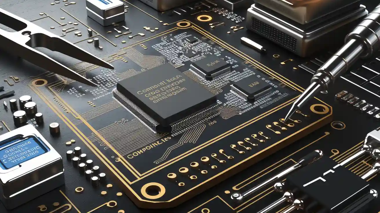
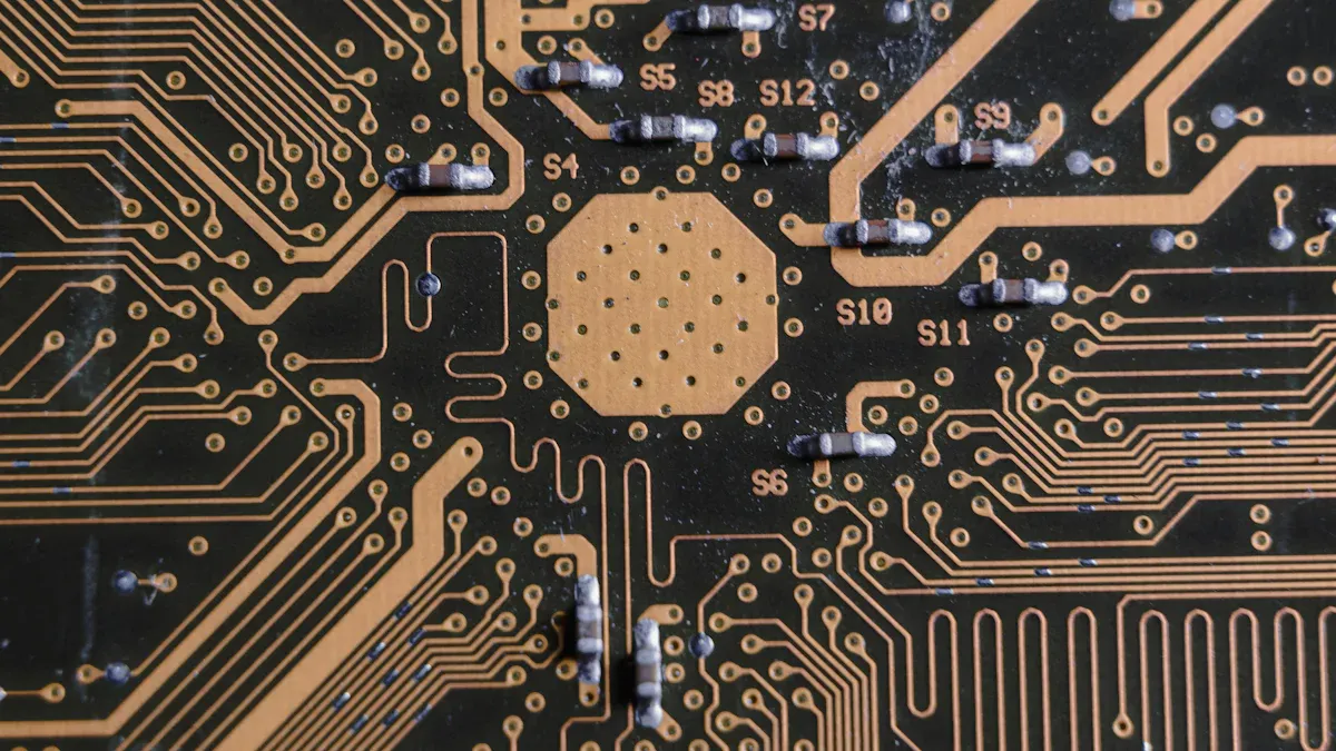
PCB silkscreen is a printed layer on a PCB. It includes text, symbols, and markings. This layer helps identify parts and guide assembly. It also ensures the board works correctly. Think of it as a map for technicians and engineers. It shows how the board is laid out.
The silkscreen layer has many uses:
Function | Description |
|---|---|
Component Identification | Shows where parts go using labels, symbols, and markers. |
Assembly Instructions | Gives clear steps for placing and soldering parts correctly. |
Aesthetics | Makes the PCB look neat, which matters for consumer products. |
Quality Control | Helps find mistakes during assembly and aids in testing. |
Additional Information | Adds part numbers, logos, and warnings to avoid errors. |
These features make assembly and testing faster and more accurate.
Common Elements Included in a Silkscreen Layer
A good PCB silkscreen has clear and helpful details. These details make assembly and inspection easier. Here are some common things you’ll see on a silkscreen:
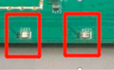
Labels like “R1” for resistors or “C1” for capacitors.
Text that is at least 1.00mm tall and 0.15mm thick.
Lines with widths between 0.10mm and 0.15mm, usually 0.12mm.
Polarity marks for parts like diodes and capacitors to show direction.
Logos or product names for branding.
Warnings and instructions to prevent mistakes during assembly.
Tip: Keep silkscreen markings away from pads or exposed copper. Leave at least 0.2mm space to avoid soldering problems.
These features improve how the PCB works and make it easier to use. For example, a company called MedTech LifeSavers had unclear silkscreen markings on a medical device. They fixed the design by adding clear labels. This helped them release a reliable product that customers praised.
Materials and Methods Used in Silkscreen Printing
The materials and methods for making silkscreens are very important. They ensure the markings stay clear and last a long time. Manufacturers use advanced techniques to make durable silkscreens.
Printing Method | Description |
|---|---|
Screen Printing | A common method using pressure or motors for quick printing. |
Inkjet Printing | A flexible option for smaller production runs. |
Special inks are also used to make strong silkscreen markings. Common inks include:
Epoxy Inks: Resist heat and moisture, making them very durable.
UV-Curable Inks: Stay clear and readable for a long time.
New technology has made silkscreen printing even better. For example:
Advancement Type | Description |
|---|---|
Laser Direct Imaging (LDI) | Allows precise and detailed silkscreen designs for dense layouts. |
Inkjet Printing | Makes it easier to create flexible and custom designs. |
Epoxy Inks | Improves resistance to environmental damage. |
UV-Curable Inks | Keeps silkscreen markings readable for the PCB’s entire life. |
Using these materials and methods, manufacturers create high-quality silkscreens for modern electronics.
The Purpose of PCB Silkscreen
Helping Identify Components
PCB silkscreen helps you find parts on a circuit board. It shows where each piece should go. Labels like “R1” for resistors or “C1” for capacitors make this easy. Without these marks, placing parts could be confusing and cause mistakes.
The silkscreen also has signs like polarity marks and pin 1 indicators. These marks help you place parts like diodes and capacitors the right way. For example, putting a diode backwards can break the whole board. Clear marks help you avoid such problems.
Here’s a simple table to compare silkscreen and solder mask:
Function | Solder Mask | Silkscreen |
|---|---|---|
Purpose | Protects and insulates | Gives visual guides |
Impact on Usability | Improves durability | Speeds up assembly |
Silkscreen markings also make assembly faster and more accurate. They work well with automated systems too.
Giving Assembly Instructions
Clear instructions are key when building a PCB. The silkscreen layer gives these instructions using labels, symbols, and grouped parts. These features show you how to place and connect parts easily.
For example, clear labels help you find parts quickly. Grouped parts make routing simpler. This setup lowers the chance of making mistakes. Imagine working on a board with many parts. Without silkscreen, you might place parts wrong. The silkscreen helps you follow the right steps, saving time.
Silkscreen marks also show where to solder and what areas to avoid. They guide you on handling delicate parts. These visual tips make assembly easier and faster.
Helping with Testing and Quality Checks
Testing and quality checks are important for making PCBs. The silkscreen helps by keeping all marks clear and correct. During testing, you can check if the silkscreen text and symbols are easy to read. This ensures you have the info needed to fix problems.
You can also check if all marks are in the right spots. For instance, missing a pin 1 mark can cause wrong connections. The silkscreen helps prevent such errors.
The silkscreen also follows industry rules for font size, spacing, and placement. This ensures the PCB meets quality standards and works well.
By helping with testing and quality checks, the silkscreen ensures you create reliable PCBs.
How PCB Silkscreen Is Applied
Overview of the Silkscreen Printing Process
Adding a silkscreen layer to a PCB takes careful steps. Each step ensures the silkscreen is clear and strong. Here’s how it’s done:
Design Preparation: Use software to plan where labels and symbols go.
Stencil Creation: Make a stencil from metal or polyester for the design.
Ink Preparation: Mix ink to get the right thickness and color.
Cleaning the PCB: Clean the board to remove dust for better ink sticking.
Screen Printing: Line up the stencil and spread ink with a squeegee.
Curing the Ink: Heat the board in an oven to harden the ink.
Inspection: Check for mistakes like smudges or misplaced markings.
Final Touches: Clean off extra ink for a neat and polished look.
These steps make sure the silkscreen is useful and looks good.
Techniques for Applying Silkscreen
Different methods are used to add silkscreen layers. For large batches, screen printing is fast and effective. It uses a stencil and squeegee to apply ink. For smaller jobs or detailed designs, inkjet printing works better. It applies ink directly without needing stencils.
A newer method, Direct Legend Printing (DLP), is also popular. It uses inkjet tools guided by software to print directly on the PCB. This method is very accurate and great for crowded layouts. Strong epoxy-based inks are often used. These inks make the silkscreen last longer and resist heat and chemicals.
Tip: Place important text carefully and use bold fonts for easy reading.
Addressing Challenges in Silkscreen Application
Adding silkscreen layers can be tricky. One problem is keeping enough space between silkscreen and pads. A gap of 6-8 mil helps avoid ink messing up soldering. Another issue is making sure lines are at least 0.1mm wide for smooth ink flow. Letters should also be taller than 0.6mm to stay clear.
Quality checks are key to fixing these problems. Regular inspections during and after printing catch mistakes early. Advanced methods like DLP help avoid errors by being precise and steady.
By solving these issues, the silkscreen layer can improve how the PCB works and looks.
Best Practices for PCB Silkscreen Design
Making Sure Text Is Easy to Read
When creating a PCB silkscreen, clear text is very important. It helps workers find parts quickly and avoid mistakes. Follow these tips to make text readable:
Use letters at least 0.8mm tall. This keeps text clear after heating or soldering.
Make lines thick enough to stay visible but not too thick. Thin lines can fade, and thick ones may hide details.
Follow rules like IPC-2221 and IPC-A-600. These ensure your silkscreen is accurate and easy to understand.
These steps help you design a silkscreen that works well and looks neat.
Smart Placement of Silkscreen Details
Putting silkscreen marks in the right spots is very important. Labels and symbols should be near the parts they describe. For example, place “R1” or “C1” close to the correct components but not on solder pads. This avoids confusion during assembly.
Group related labels together. For example, keep labels for connected parts in the same area. Don’t put markings too close to the PCB edges. This prevents damage over time.
Good placement makes the PCB easier to use and improves its appearance.
Keeping the Design Simple and Clear
Crowded silkscreen designs can confuse workers and cause mistakes. Overlapping marks can hide important details. A clean design makes everything easy to see and understand.
In a PCB with many layers, too much information can overlap. This makes some details hard to read because they share the same space.
Leave enough space between silkscreen marks. Keep at least 0.2mm between text and solder pads. This stops ink from causing soldering problems. Remove extra text or symbols to simplify the design. A clean silkscreen is easier to use and looks better.
Using Standardized Symbols and Fonts
Using standard symbols and fonts makes PCB silkscreens clear. It helps technicians assemble and test boards without confusion. Following these rules lowers mistakes, even in tricky layouts.
Here are some simple tips:
Fonts: Use bold sans-serif fonts for clear and sharp text.
Text Size: Keep letters at least 30 mils (0.762 mm) tall. For better reading, aim for 40-50 mils (1.016-1.27 mm).
Line Width: Make text lines 5-8 mils (0.127-0.203 mm) wide. This keeps them readable and avoids smudging.
Spacing: Leave at least 10 mils (0.254 mm) between text and pads. This stops overlapping and keeps the design neat.
Tip: Test your silkscreen on a sample board to check clarity after production.
Symbols are also very important. Polarity marks like “+” and “-” show how to place parts like capacitors. Pin 1 markers on ICs stop placement errors. Using common symbols makes the layout easy for everyone to understand.
By following these steps, your silkscreen will look neat and work well. A good silkscreen shows care and makes the PCB easier to use.
Why PCB Silkscreen Is Critical for Assembly
Reducing Errors and Miscommunication
PCB silkscreen helps reduce mistakes during assembly. It shows clear labels to identify and place parts. Labels like “R1” for resistors or “C1” for capacitors show where parts go. Polarity marks and pin indicators stop parts from being placed wrong. Incorrect placement can damage the board or make it fail.
The silkscreen also helps team members avoid confusion. Standard symbols and instructions ensure everyone follows the same steps. This reduces errors during assembly.
Silkscreen helps find and place parts correctly.
It gives clear instructions for placing and soldering parts.
It highlights mistakes for quick fixes during quality checks.
These features make silkscreen important for making reliable electronics and avoiding costly errors.
Enhancing Assembly Efficiency
A good PCB silkscreen makes assembly faster. Clear labels and symbols help you find parts quickly. This saves time, especially on boards with many components. Grouped labels and neat layouts make the process even easier.
Silkscreen markings also help machines during automated assembly. Machines use these marks to place parts correctly. Without them, the process would slow down and have more mistakes. By helping both people and machines, silkscreen speeds up production and improves quality.
Improving Collaboration Between Designers and Technicians
The silkscreen helps designers and technicians work together better. Designers use it to show their plans clearly. Technicians use it to assemble the board correctly. Standard symbols and fonts make communication easy and avoid confusion.
For example, designers add polarity marks or pin indicators to guide technicians. These details ensure the board works as planned. By improving teamwork, the silkscreen helps create high-quality boards that meet customer needs.
PCB silkscreen is important for easier and accurate assembly. It shows where parts go, lowers mistakes, and helps with quality checks. Using good silkscreen design makes assembly faster and more reliable. This improves how the PCB works and ensures it performs well in real use. A clear silkscreen shows careful planning and helps your project succeed.
FAQ
What is the smallest text size for PCB silkscreen?
The smallest text size for PCB silkscreen is 0.8mm tall. This size keeps the text readable after soldering and heating. For clearer text, use a size of 1.0mm or more.
Can silkscreen touch solder pads?
No, silkscreen should not touch solder pads. Keep at least 0.2mm space between them. This avoids soldering problems and keeps markings clear during assembly.
What ink is used for PCB silkscreen?
Epoxy and UV-curable inks are used for PCB silkscreens. These inks resist heat, water, and chemicals. They stay strong and readable for the PCB’s life.
Why are polarity marks needed on PCB silkscreen?
Polarity marks show how to place parts like diodes and capacitors. If placed wrong, these parts can harm the PCB or make it fail. Clear marks help avoid such mistakes.
Do silkscreen markings help machines in assembly?
Yes, silkscreen markings help machines during assembly. Labels and symbols guide machines to place parts correctly. This reduces mistakes and speeds up the process.