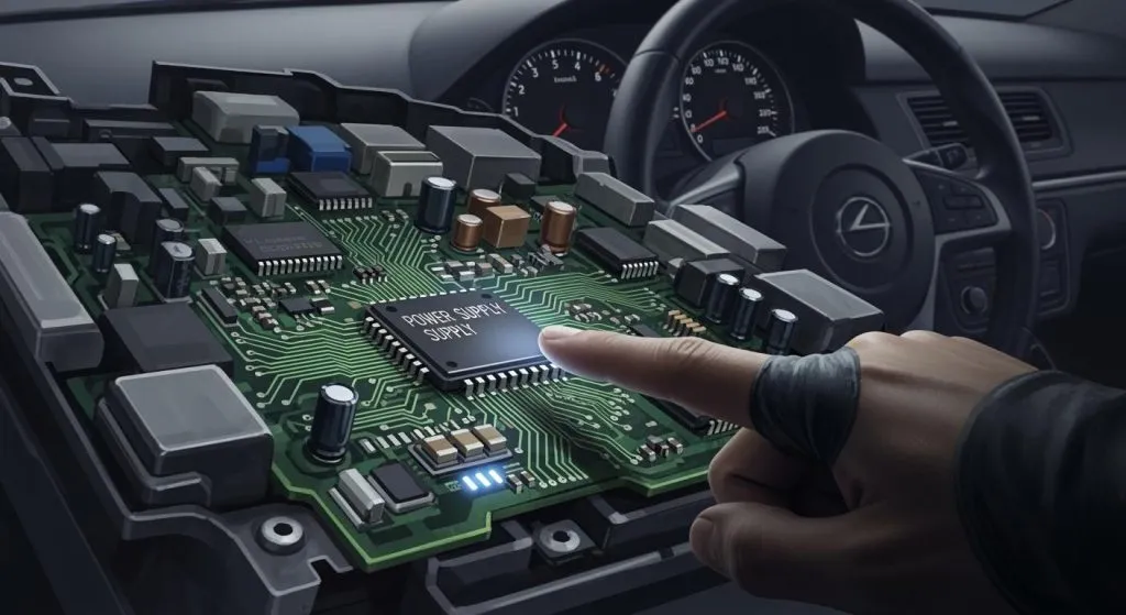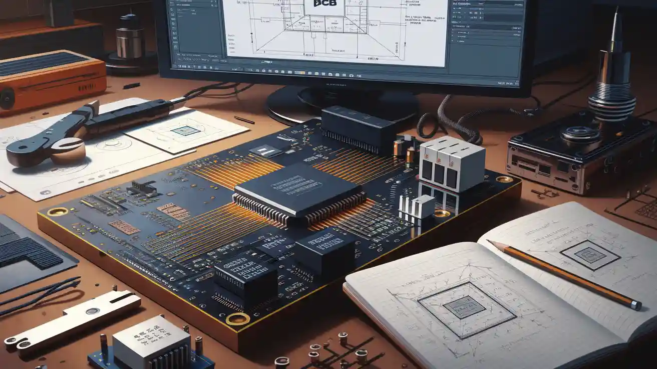
IC board (pcb) design affects how devices work and last. Every ic board design starts with a printed circuit board. This board is the backbone for ic components. The pcb design process changes how well it works, how long it lasts, and the price. Printed circuit board choices affect where ic parts go and how they connect. These choices change how well the device works. Engineers in ic board design care about reliability and saving money. This helps them make better electronic devices. Teams use good design ideas and new ic inventions. This helps them get the best results.
Key Takeaways
A good PCB design makes devices work better and last longer. It also helps save money. Engineers begin by looking at what the device needs. They pick the right parts for the job. EDA tools and simulation help spot mistakes early. This lets engineers fix problems before building the board. Good PCB layout and routing help control heat. They also guide signals and power the right way. This gives better results. Keeping signal and power strong stops mistakes. It also helps devices last longer. Thermal management keeps the board safe from heat. This makes the board last more years. Designing for manufacturability makes building easier. It also gives better quality products. Learning about new technology and methods helps engineers improve PCB designs.
Printed circuit board basics
What is a printed circuit board
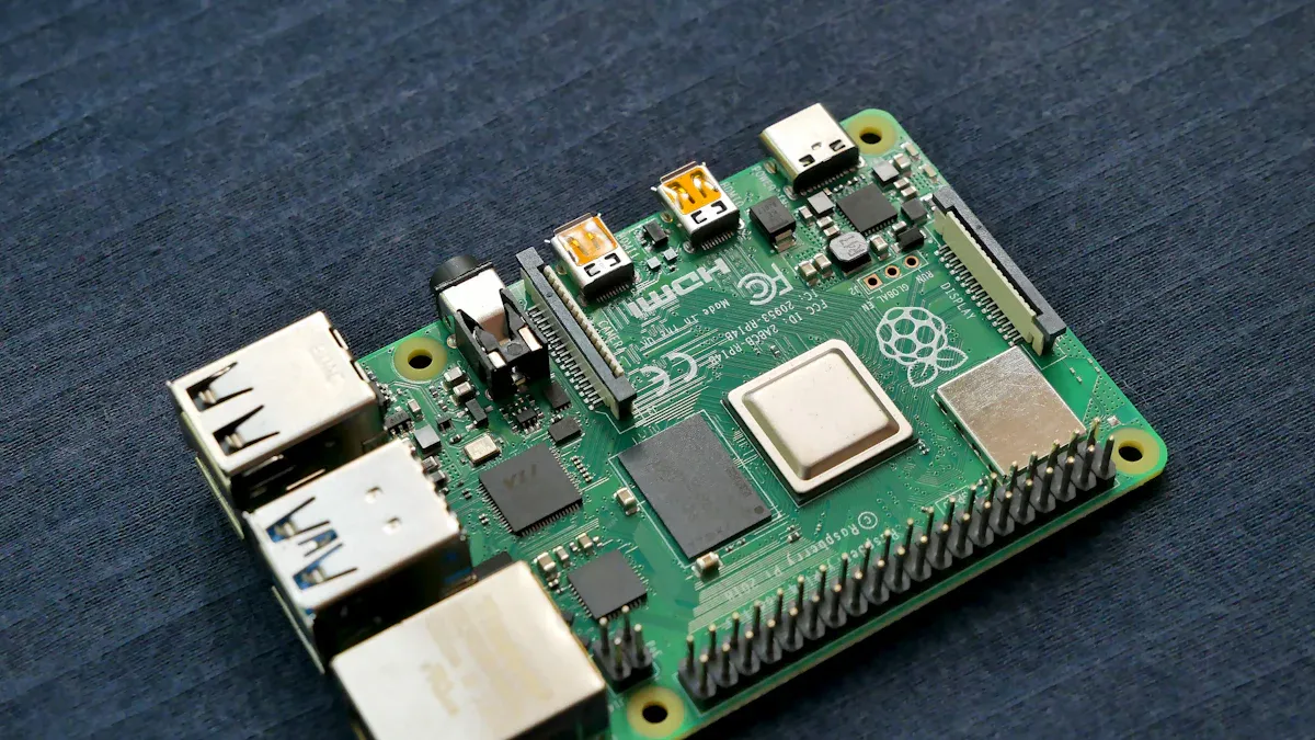
A printed circuit board, or PCB, is found in most electronics. Engineers use a PCB to hold and connect parts. The board has copper lines that act like roads for electricity. These lines let electricity move between the parts. How a PCB is made decides how the circuits work together. A good PCB layout keeps things neat and easy to follow. This helps people build and fix the device.
PCBs can be many shapes and sizes. Some have one layer, but others have more layers stacked up. More layers make the circuit more complex. Engineers pick the best PCB layout for each device. They think about how the circuits will fit and work.
Note: A good PCB layout can stop mistakes and help the device work better.
Why PCB design matters
PCB design is important for how devices work. The layout changes how electricity moves in the circuits. If the design is bad, the circuits might not work right. This can break the device. Engineers must plan the PCB layout with care. They check how each circuit links to the others. They also think about where to put each part.
A strong PCB design stops problems like short circuits or signal loss. It also makes the device safer. Good design can lower the cost to make the device. It can also help the device last longer.
Good PCB layout helps the device work better.
Careful design makes the device more reliable.
Smart layout choices can save money.
Performance and reliability
Performance and reliability are big goals in PCB design. How engineers set up the PCB layout changes how well the device works. A good layout keeps circuits short and simple. This lowers the chance of signal trouble. It also helps control heat, which can hurt circuits.
Reliability means the device works well for a long time. Engineers test the PCB layout to find weak spots. They use special tools to see if the circuits can handle stress. They also look for ways to make the design better.
Factor | Impact on PCB |
|---|---|
Layout | Changes performance |
Makes it more reliable | |
Component choice | Helps the circuits |
Engineers try to balance performance and reliability. They change the PCB layout when new technology comes out. This keeps devices safe and working well.
IC board (pcb) design process
Requirement analysis
The ic board (pcb) design process begins with requirement analysis. Engineers gather all the details about what the device must do. They look at the functions, size, and power needs. This step sets the stage for every other part of ic board design.
Component selection
Engineers choose the right ic parts for the circuit. They check the voltage, current, and speed for each ic. The choice of components affects the pcb layout and the way circuits connect. Good component selection helps the ic board design meet performance goals. Engineers follow strict guidelines to avoid mistakes. They also think about cost and how easy it is to get each ic.
Engineers list all needed ic parts.
They check if each ic fits the design.
They compare different options for the best match.
Topology and interfaces
Next, engineers decide how the ic parts will connect. They plan the topology, which shows the flow of signals in the circuit. The interfaces link the ic board to other devices. A clear topology helps with pcb layout and routing. Engineers use guidelines to keep the design simple and reliable.
Tip: A well-planned topology makes routing easier and reduces errors in the circuit.
Schematic design
After requirement analysis, engineers move to schematic design. This step creates a map of the circuit. The schematic shows how each ic connects to others. It acts as a blueprint for the pcb layout.
EDA tools
Engineers use EDA (Electronic Design Automation) tools to draw the schematic. These tools help them place each ic and wire in the right spot. EDA tools also check for errors in the circuit. They follow guidelines to make sure the design is correct. The tools help engineers plan the pcb layout and routing before making the real board.
EDA Tool Feature | Benefit for ic board design |
|---|---|
Error checking | Finds mistakes early |
Auto-routing | Speeds up pcb layout |
Simulation | Tests circuit performance |
Simulation
Simulation lets engineers test the circuit before building it. They use EDA tools to run these tests. Simulation checks if the ic board design meets all requirements. It finds problems with signal flow, power, and heat. Engineers adjust the schematic and pcb layout based on simulation results. This step saves time and money by catching errors early.
PCB layout
The pcb layout step turns the schematic into a real board. Engineers place each ic and wire on the pcb. They follow guidelines to make sure the layout works well. Good pcb layout improves performance and makes routing easier.
Board size and placement
Engineers pick the right size for the pcb. They arrange each ic to fit the space. The placement of parts affects routing and the way circuits work. A compact layout can lower costs and boost performance. Engineers use guidelines to avoid crowding and to keep the board easy to build.
Place high-speed ic parts close together.
Keep power and ground lines short.
Leave space for routing and testing.
Thermal and electrical factors
Heat and electricity affect how the pcb works. Engineers plan the layout to control heat. They use wide traces for high current and add extra copper for cooling. Good pcb layout keeps circuits safe from overheating. Engineers also check for electrical noise and signal loss. They follow guidelines to protect the ic and the whole circuit.
Note: Careful planning of thermal and electrical factors in pcb layout increases the life of the ic board.
Routing
Routing is a very important step in pcb design. Engineers use routing to link all the parts on the pcb. They plan where the signals and power lines will go. Good routing helps the pcb work well and last longer. Engineers must follow strict rules when they do routing. They do not use sharp corners and keep traces short. This helps keep signals strong and lowers mistakes.
Routing choices change the whole pcb layout. Engineers pick trace widths based on how much current flows. They keep fast signals away from sensitive analog lines. This stops interference and keeps signals clear. Routing also makes it easier to build the pcb. Simple routing paths help avoid mistakes when making the board.
Signal integrity
Signal integrity is very important during routing. Engineers work to keep signals clean and free from noise. They use special traces to protect signal integrity. Matching impedance stops signal loss and reflections. Engineers space traces apart to lower crosstalk. Crosstalk can make unwanted signals in other traces.
Engineers use simulation tools to check signal integrity before finishing the pcb layout. They look for places where signals might get weak. If they find problems, they change the routing or layout. This makes sure the pcb has strong signal integrity. Good signal integrity means the device works better and has fewer errors.
Tip: Always check the pcb layout for signal integrity problems before making the board.
Power delivery
Power delivery is very important in pcb layout and routing. Engineers use wide traces for power lines to carry more current. They put decoupling capacitors close to ic pins. This helps stop voltage drops and noise. Good power delivery keeps the pcb working well.
Engineers use many ground and power planes in multilayer pcb designs. These planes lower resistance and help power integrity. They also help move heat away from hot spots. Careful routing of power lines stops hot spots and voltage dips. Engineers check the layout to make sure all parts get steady power.
Focusing on power delivery during routing helps the pcb work well and last longer. It also makes the pcb easier to test and build.
Simulation and verification
Simulation and verification help engineers find problems before making the pcb. They use simulation tools to test the pcb layout in real situations. These tools check how signals and power move across the pcb. Engineers test for signal integrity, power integrity, and heat problems.
Simulation results help engineers change the pcb layout. If a test shows weak signals, engineers change routing or trace width. They also check for power delivery problems. Verification steps make sure the pcb layout meets all design goals. This saves time and money by lowering mistakes before making the board.
Electrical and thermal checks
Electrical and thermal checks are a big part of simulation and verification. Engineers use these checks to find weak spots in the pcb. Electrical checks look for shorts, opens, and impedance problems. They also test for signal integrity issues.
Thermal checks look for heat buildup in the pcb layout. Engineers use simulation tools to find hot spots. They add thermal vias or copper pours to help heat move away. These steps protect the pcb from getting too hot during use.
Note: Electrical and thermal checks help the pcb last longer and work better.
Manufacturing and testing
Manufacturing and testing turn the pcb layout into a real product. Engineers get the pcb layout ready for production by making detailed files. These files guide the building process and help keep things correct.
Production files
Production files include Gerber files, drill files, and assembly drawings. Engineers make these files from the pcb layout. Each file gives instructions for a different step in making the board. Clear and correct files help avoid mistakes and speed up the process.
Engineers check all production files before sending them to the factory. They look for missing details or errors. This check helps stop costly mistakes during manufacturing.
Fabrication
Fabrication turns the pcb layout into a real board. Factories use the production files to build the pcb layer by layer. They etch copper traces, drill holes, and add solder masks. Each step follows the design in the pcb layout.
Quality control checks happen during fabrication. Factories look for defects or layers that do not line up. They use machines to compare the finished pcb to the original layout.
Post-production tests
Post-production tests make sure the pcb works as planned. Engineers use machines to check for shorts, opens, and signal problems. They also test power delivery and heat performance.
Testing helps find problems missed in earlier steps. Engineers fix any issues before making more boards. This makes sure every pcb meets quality standards.
Reminder: Careful testing after making the pcb helps protect the final product’s reputation.
IC board design principles
Signal integrity
Signal integrity is a key part of IC board design. Engineers work hard to keep signals clean and strong. This helps the device work well and last longer. If signal integrity is bad, the device can have errors or stop working. Engineers use smart design to protect signal integrity.
A good layout keeps traces short and straight. Engineers do not use sharp corners or sudden trace changes. They keep high-speed signals away from sensitive analog signals. This lowers noise and keeps signals steady. Simulation tools help engineers check signal integrity before making the board. These tools show where signals might get weak or noisy.
Note: High-speed circuits often have signal integrity problems. Early checks help stop expensive mistakes.
Impedance and crosstalk
Impedance control is important for signal integrity. Engineers match trace impedance to the source and load. This stops reflections that can weaken signals. Controlled impedance keeps the circuit working well. Engineers use special tools to find the right trace width and spacing.
Crosstalk happens when signals in one trace affect another trace. Engineers space traces apart to lower crosstalk. They use ground planes to shield signals. Good design keeps crosstalk low and protects signal integrity. Engineers check for crosstalk during simulation and change the layout if needed.
Factor | Impact on Signal Integrity |
|---|---|
Impedance | Stops reflections |
Crosstalk | Lowers noise |
Trace length | Keeps signals strong |
Engineers use these ideas to keep signal integrity high and make the device more reliable.
Power integrity
Power integrity means power flows steady across the board. Engineers design power delivery to keep voltage steady and lower noise. Good power integrity helps the device work well and last longer. Bad power integrity can cause voltage drops, noise, or device failure.
Engineers use wide traces and solid ground planes in the layout. They put decoupling capacitors close to IC pins. These steps keep power steady and help the circuit work well. Simulation tools help engineers check power integrity before making the board.
Noise reduction
Noise reduction is a big part of power integrity. Engineers use careful layout to keep noise away from sensitive signals. They keep power and ground planes apart to lower noise. Decoupling capacitors filter out high-frequency noise. Good design keeps noise low and helps the device work better.
Tip: Put decoupling capacitors as close as you can to each IC pin for best noise reduction.
Engineers check for noise problems during simulation. They change the layout to fix any issues. This focus on noise reduction helps the device work well and last longer.
Thermal management
Thermal management keeps the IC board safe from heat. Engineers design the layout to move heat away from hot spots. Good thermal management keeps the device safe and helps it last longer. Bad thermal management can make circuits fail or lose performance.
Engineers use wide copper areas and thermal vias in the layout. These features help spread heat across the board. They put hot parts away from each other to lower heat buildup. Simulation tools help engineers check thermal performance before making the board.
Heat dissipation
Heat dissipation is a main goal in thermal management. Engineers design the layout to let heat escape fast. They use heat sinks, copper pours, and thermal vias to move heat away from ICs. Good heat dissipation keeps the board cool and helps it work well.
Thermal Feature | Benefit for Performance |
|---|---|
Copper pours | Spread heat |
Thermal vias | Move heat to other layers |
Heat sinks | Pull heat away from ICs |
Reminder: Good thermal management in the layout makes the device more reliable and keeps it working well.
Engineers use these design ideas to protect the IC board from heat and help it work better.
EMC
Electromagnetic compatibility (EMC) makes sure an IC board works well. It helps the board not cause or get unwanted electrical noise. Engineers care about EMC to keep circuits safe and working right. Good EMC design helps devices pass tests and work well in real life.
EMI control
Electromagnetic interference (EMI) can mess up signals and hurt device performance. Engineers use different ways to control EMI and keep circuits steady. They plan the PCB layout to make loop areas small. They also avoid long parallel traces. Shorter traces help stop noise from leaving the board.
Shielding is important for EMI control. Engineers add ground planes and shielding boxes to block bad signals. They use ferrite beads and filters to stop high-frequency noise. Careful part placement and routing lower EMI risk even more.
Tip: Put decoupling capacitors close to IC pins. This blocks high-frequency noise and helps the board work better.
Engineers test boards for EMI while designing. They use simulation tools to find problem spots and fix the layout. These steps help the product meet EMC rules and work well in many places.
Manufacturability
Manufacturability means making the IC board easy for factories to build. Engineers think about manufacturability early to avoid costly changes later. A board that is easy to make also works better and lasts longer.
Production efficiency
Production efficiency shows how fast and smooth a factory can make the board. Engineers use standard part sizes and clear labels to help. They do not put parts too close together. This makes assembly and checking easier.
A good board uses simple routing and smart part placement. This lowers mistakes during building and testing. Engineers pick materials and steps that fit what the factory can do. These choices keep costs down and help the board work well.
Manufacturability Factor | Impact on Production Efficiency |
|---|---|
Standard part sizes | Faster assembly |
Clear labeling | Fewer errors |
Logical layout | Easier inspection |
Simple routing | Lower risk of defects |
Note: Good manufacturability makes production faster. It also helps the device work well and last longer.
Engineers check the design with factory teams before finishing the board. This teamwork finds problems early and helps the board meet both performance and production needs.
PCB technology trends
Multilayer boards
Multilayer boards have changed how engineers build electronics today. These PCBs have many layers of copper and insulation. Each layer carries signals or power for the device. This design lets engineers put more circuits in less space. Devices like smartphones and computers use these boards for hard jobs.
Engineers pick multilayer PCBs to make devices work better. More layers help with signal paths and lower interference. High-speed circuits often need these boards. The extra layers guide signals and cut down on noise. Multilayer boards also help with power delivery. They keep voltage steady all over the device.
Note: Multilayer PCBs help make small and strong devices.
HDI technology
HDI technology means High-Density Interconnect. This uses very thin lines and tiny holes called microvias. HDI PCBs fit more connections in a small area. Engineers use HDI to make devices lighter and thinner.
Phones, tablets, and wearables use HDI PCBs. These boards handle fast signals and quick data moves. HDI trends show more devices need faster and smaller PCBs. Engineers pick HDI to save space and boost how well things work.
HDI boards also help keep signals strong. Shorter paths and tiny parts lower signal loss. This makes HDI great for high-speed circuits. Engineers often use HDI with multilayer boards for the best results.
Feature | Benefit |
|---|---|
Microvias | Save space |
Thin traces | Support high-speed |
Dense layout | Fit more circuits |
Flexible PCBs
Flexible PCBs can bend and twist without breaking. Engineers use these boards in things that move or fold. Wearables, medical tools, and cameras often need flexible PCBs. These boards fit in tight spots and odd shapes.
Flexible PCBs use thin plastic for the base. This lets the board bend many times. Engineers design flexible PCBs for simple or hard circuits. Some devices mix stiff and bendy parts. This gives both strength and flexibility.
Flexible PCBs help lower weight and size. They also make building easier. As tech moves to smaller and smarter things, flexible PCBs get more popular. Engineers think flexible boards are key for future pcb ideas.
Tip: Flexible PCBs are good for products that move or change shape.
RF and high-speed
RF and high-speed technology are very important in today’s PCB design. Engineers use them in things like smartphones and Wi-Fi routers. They are also used in new medical machines. RF circuits work with signals that move very fast. High-speed circuits move data quickly and need careful planning.
Many new ideas try to make RF and high-speed circuits better. Engineers must stop signal loss and noise. They pick special materials and follow layout rules. This keeps signals strong. High-speed circuits need short and straight paths for signals. This helps stop mistakes and keeps data moving fast.
Engineers use controlled impedance traces for high-speed signals. These traces help keep the signal shape the same. Ground planes protect signals from noise. In RF designs, engineers do not use sharp corners or long parallel traces. These steps help lower signal loss and crosstalk.
Note: Good RF and high-speed design lets devices send and get data without mistakes.
Many devices use both RF and high-speed circuits now. For example, a smartphone uses RF for wireless signals. It uses high-speed circuits for fast data. Engineers must balance both in one PCB. They keep RF and high-speed parts apart on the board. This keeps signals clean and stops them from mixing.
Engineers test RF and high-speed circuits with simulation tools. These tools show how signals move on the board. If they find a problem, they change the layout or materials. Sometimes they use special coatings or shields to protect signals.
The table below shows some main steps in RF and high-speed circuit design:
Step | Purpose |
|---|---|
Controlled impedance | Keeps signals steady |
Ground planes | Shields against noise |
Short signal paths | Reduces signal loss |
Simulation | Finds and fixes problems |
Engineers follow strict rules for high-speed circuit design. They check every trace and connection. This careful work helps devices keep up with new technology. As tech grows, RF and high-speed circuits will be even more important in new products.
Continuous learning
Staying updated
Engineers in PCB design need to learn new things often. Technology changes fast. New materials and tools come out every year. Engineers read news and talk in online groups. Many go to workshops or watch webinars to learn new design tips. Some follow experts on social media for quick news.
Tip: Learning all the time helps engineers fix problems early and find better ways to work.
A good engineer checks for updates in design software. They also look at new safety rules and test steps. This habit keeps their skills strong and their work up to date.
Advanced methods
Modern PCB design uses special ways to solve hard problems. Simulation tools let engineers test circuits before building them. These tools show how heat, signals, and power move on the board. Engineers use 3D modeling to see how parts fit together. This step helps them stop mistakes before making the real board.
Some teams use machine learning to guess design problems. Others use automatic checks to find errors quickly. These new ways save time and make the work better. They also help different parts and systems work together.
A table below shows some advanced methods and their benefits:
Method | Benefit |
|---|---|
Simulation tools | Find problems early |
3D modeling | Improve part fitting |
Automated checks | Reduce human error |
Machine learning | Predict design issues |
Engineers who use these ways can do hard projects. They make sure each design is very good.
Industry adaptation
The electronics industry changes quickly. Companies must change to keep up. They update how they design to meet new needs. Many try new materials or layouts for better results. Teams test if their boards work with new devices and standards.
Engineers work with other teams to share ideas. They join groups to learn the best ways to design. This teamwork helps everyone get better at their job. Companies that change fast can make better products and help customers.
Note: Changing with the industry keeps products safe, strong, and ready for what comes next.
To get really good at IC board PCB design, you need to know the steps and rules well. Engineers who use clear steps and smart ideas make devices that work well and last long. They keep learning about new technology and ways to design so their skills stay strong.
Trying new ideas and using what works best helps teams make better products. Winning at PCB design means using what you know, learning more, and making good choices.
FAQ
What is the main purpose of a PCB in electronic devices?
A PCB holds and connects electronic parts. It gives circuits a strong base. Engineers use PCBs to keep parts neat. PCBs make sure electricity flows the right way.
How do engineers choose the right PCB material?
Engineers pick materials by looking at heat, speed, and price. FR-4 is used for most boards. Some fast or bendy boards need special materials.
Why do multilayer PCBs improve performance?
Multilayer PCBs fit more circuits in a small space. They help stop signal problems and make signals better. Devices that are fast or complex use extra layers.
What tools help engineers design PCBs?
Engineers use EDA tools for design work. These tools help draw, plan, test, and check for mistakes. Altium Designer, Eagle, and KiCAD are popular choices.
How do engineers prevent overheating on a PCB?
Engineers use wide copper lines, thermal vias, and heat sinks. They keep hot parts apart and add copper to spread heat. Simulation tools help find hot spots.
What is signal integrity, and why does it matter?
Signal integrity means signals stay strong and clear. Good signal integrity stops mistakes and keeps devices working. Engineers use short lines and set impedance to protect signals.
Can flexible PCBs replace rigid boards in all devices?
Flexible PCBs are good for things that bend or move. They cannot replace rigid boards in every device. Some devices need the strength of rigid PCBs.