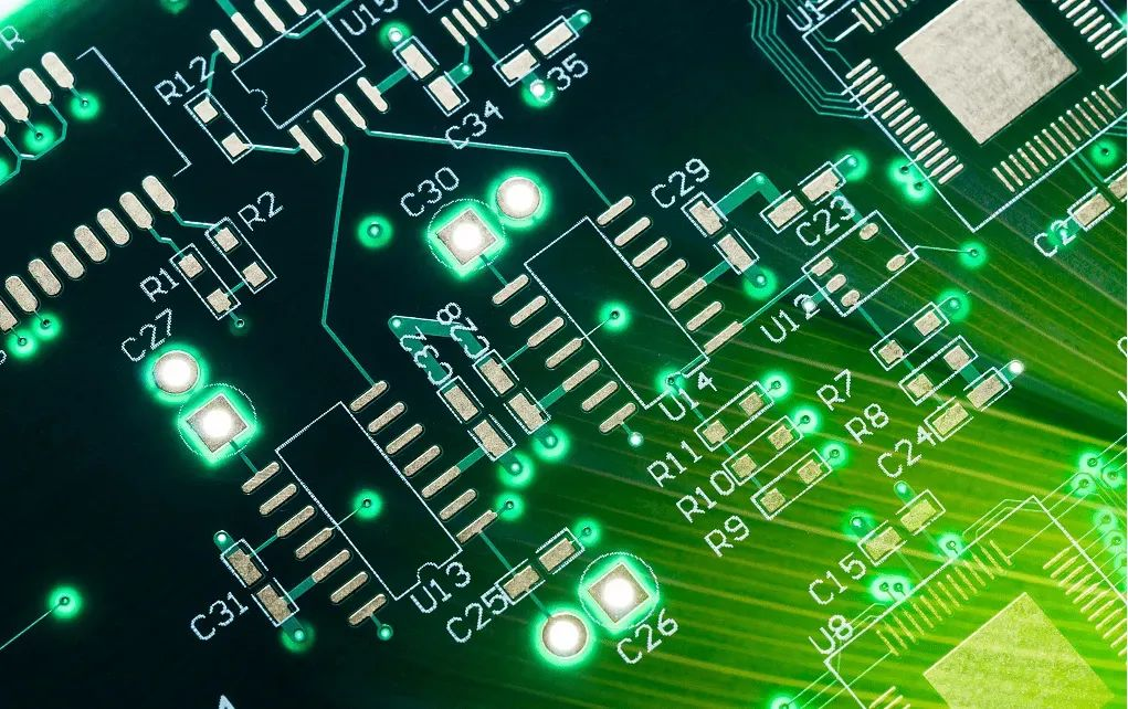
8 Safety Distances That Must Be Considered in PCB Design
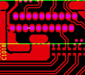
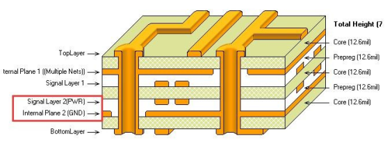
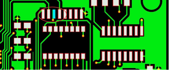
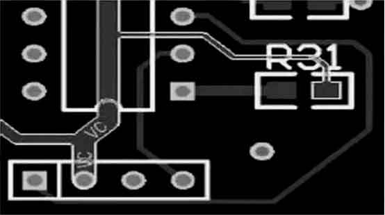
There are many safety distance considerations in PCB design, including spacing between traces, character spacing, pad spacing, and more. Here, we classify them into two categories: electrical-related safety distances and non-electrical-related safety distances. 01 Electrical-Related Safety Distances Trace-to-Trace Spacing For the processing capabilities of mainstream PCB manufacturers, the minimum distance between traces should not be […]
8 Safety Distances That Must Be Considered in PCB Design Read More »