A via in pad places a plated hole inside or directly on a component land pattern, routing signals or heat away from fine-pitch parts. In a filled and capped via, the barrel holds resin or conductive material, and plated copper seals the top. You get a flat, solderable pad surface.
That flatness matters. Open barrels wick solder, trap air, and cause voids or head-in-pillow defects during reflow. Good pcb via-in-pad design prevents these failures. This post gives you a direct framework for via-in-pad design decisions: when filled and capped vias are the right call, when simpler structures suffice, and which cost factors drive the choice. Use it to settle your via in-pad design questions before layout starts.
Key Takeaways
Use filled and capped vias under fine-pitch BGA, CSP, and thermal pads for reliable solder joints.
Skip via-in-pad when the pad has room for standard routing or when small chip parts sit nearby.
Specify IPC-4761 Type VII in fab notes to ensure proper filling and capping.
Keep the via barrel completely filled and the copper cap flat to prevent solder voids.
Avoid open or tented vias in solder pads because they trap air and cause defects.
Ask your fabricator about fill materials, cap thickness, and inspection methods early.
Apply filled and capped vias only where solder paste meets the hole to control costs.
Inspect via-in-pad quality with X-ray and cross-sections to catch hidden defects.
What Via-in-Pad Means for Assembly
Definition and Purpose
A via in pad is a plated hole placed inside or directly on a component land pattern. You use this structure when conventional fanout routing cannot reach the pad. Standard dog-bone breakout needs space beside the pad for a short trace and a via. Fine-pitch parts remove that space. The via in the copper landing pad solves the routing problem by moving the connection point under the component itself.
The purpose is simple. The via carries a signal or heat away from the part without stealing routing area around it. That single change frees space on dense boards and shortens the electrical path. Assembly then depends on one condition: the pad surface must stay flat and solderable.
The Assembly Problem It Solves
An open via barrel creates three assembly problems. First, solder wicks into the hole during reflow. The paste flows away from the joint and leaves the connection starved. Second, air trapped in the barrel expands and pushes through the molten solder. The result is a void inside the joint. Third, escaping air can eject solder and form solder balls on the board surface.
These defects are hard to see and harder to rework. A void weakens the joint. A head-in-pillow defect can pass initial inspection and fail in the field. Proper via filling and capping close the barrel before assembly starts. The cap gives the paste a solid surface to wet against, so the joint forms where you designed it.
Where It Appears on Modern Boards
You will find via in pads most often under fine-pitch BGA and CSP packages. Inner rows on these parts leave no room for dog-bone fanout. LGA sites show the same constraint. Exposed thermal pads are another common location. A thermal pad needs a flat, solderable surface, and open vias under it would drain paste away.
The pattern is consistent. Via-in-pad design appears wherever pad density outruns routing space. That covers high-density boards, high-speed paths that need a short vertical drop to a plane, and thermal interfaces. The package list matters less than the constraint. If the pad has no room for standard breakout, the via moves into the pad.
Tented, Plugged, Filled, and Capped Vias
Four via structures appear in fabrication notes, and they differ in how much of the barrel they close. You need to match the structure to the pad, not to habit. The three subsections below separate the simple closures from the solderable ones.
Tented and Plugged Vias
Tenting covers the via opening with solder mask. The barrel stays open underneath. Plugging pushes material partway into the hole, usually from one side, and the closure stops short of a full fill. Both options cost less than a full treatment, and both suit vias that sit outside solder pads.
Tented and plugged vias fit best on ordinary signal vias, test points, and any hole that never meets paste. They fail when you place them in a pad. A via tented on both sides without filling traps air pockets, and that air expands during reflow. The same risk applies to a via filled but not properly capped. Material sits below the pad surface, air remains, and defects follow.
Filled Versus Capped
Via filling pushes material through the barrel until the hole is solid. Capping adds plated copper over the filled barrel and planarizes the surface. Filling alone leaves a dimple or a soft resin surface. A copper cap restores a flat, solderable land.
The distinction drives your specification. Resin-filled and copper-capped vias give you a surface that solder paste wets evenly. A capped via in pad also survives planarization without concavity, which matters under fine-pitch parts. Use filled-only structures where the via needs sealing but not soldering. Reserve the full capped and filled stack for pads that carry paste.
IPC-4761 Type VII and VIPPO
IPC-4761 defines via protection types, and Type VII describes a via filled and covered with a plated cap. The industry also calls this via-in-pad plated over, or VIPPO. You will see pofv or vippo construction written in fab notes as shorthand for the same requirement.
Specify the type by name in your documentation. A note that says “fill vias” leaves room for interpretation, and pcb via filling without a cap requirement may return a dimpled pad. State IPC-4761 Type VII, name the layer pairs, and confirm the copper cap thickness with your fabricator. That clarity protects both the via-in-pad design intent and your assembly yield.
How the Fill and Cap Process Works
Fill Materials: Resin Versus Conductive
The fill material decides how the barrel behaves after cure. A non-conductive resin fills the hole and seals it against air and chemistry. A conductive paste adds electrical continuity through the barrel. Both approaches support via filling, and both need a complete fill to work.
Compare copper paste vs. electroplated copper filling when you weigh conductivity against process complexity. Paste fills faster and suits small holes. Electroplated copper builds a solid metal plug and matches the barrel’s thermal expansion closely. Filling the via with a conductive epoxy is another option for heat paths and ground connections. Discuss the choice with your fabricator early, because the material drives the downstream copper cap plating recipe.
A complete fill reduces void risk and improves plating consistency. Material must reach the bottom of the barrel without gaps. Partial fills leave air pockets that expand during reflow and push through the cap.
Capping and Planarization
After via filling, the board moves to planarization. The fabricator grinds or mills the excess material flush with the pad surface. A flat surface lets you cap the via without a dish or dimple.
Copper capping follows. The process builds plated copper over the filled barrel, and this plating over with copper restores a continuous land. A resin-filled and copper-capped via gives you a surface that solder paste wets evenly. Control the copper cap thickness and the cap diameter, since both affect joint formation under fine-pitch parts.
Process Controls That Affect Yield
Yield depends on discipline at every step. Drill quality, fill pressure, cure profile, and copper cap plating all interact. A weak fill shows up later as a void under X-ray. Poor planarization shows up as concavity that traps flux.
Not every hole needs the full stack. Drilled vias of 0.3 mm or less are often filled and shut with solder mask when a full solderable cap is not required. That choice saves cost on holes that never meet paste. Apply full via-in-pad filling only where a via in pad carries solder. A good pcb via filling guide from your fabricator will list their fill materials, cap tolerances, and inspection limits. Follow it during via-in-pad design, and confirm the pcb via filling notes in your fab file before release.
When to Use Via in Pad
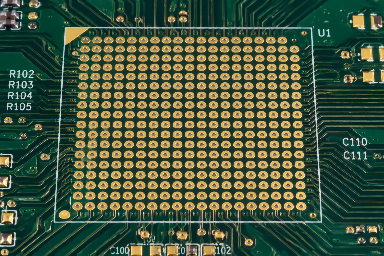
Three conditions justify moving a via into the pad. Each one removes the space or the surface that standard routing needs. Read your layout against these cases before you commit to the structure.
Fine-Pitch BGA, CSP, and LGA
Tight pin pitch creates the clearest case. A fine-pitch BGA leaves a narrow channel between ball pads. Inner rows sit behind outer rows, and a dog-bone breakout needs a trace plus a via beside each pad. That geometry does not fit. The via must move under the pad, and once it sits there, the pad needs a flat, sealed surface for assembly.
CSP and LGA sites follow the same logic. The pin pitch or the pad arrangement removes the escape path. You face a choice: drop to a finer line width, add layers, or place the via in the pad. The last option often costs less than the first two. This is where bga and via-in-pad applications concentrate, and where the assembly risk is highest. A void under a fine-pitch ball is difficult to inspect and costly to rework.
Check the datasheet land pattern first. Many package guides already assume a via in pad for inner rows. Follow that guidance, and confirm the fill and cap requirement with your fabricator before release.
High-Density and High-Speed Designs
Density drives the second case. Placing vias under pads saves routing area. That saving lets you reduce layer count or shrink board size. Both changes cut cost across the whole product, not just the via process. A dense board with no breakout room forces the decision anyway. A board with some room still benefits when the via under the pad frees a channel for another net.
High-speed paths add a separate reason. A via in pad gives a direct vertical drop to an internal ground or power plane. That short path lowers loop inductance and improves signal integrity. The same logic applies to a bypass capacitor placed close to the pin. A vertical connection to the plane beats a lateral trace with a stub.
These via-in-pad designs reward you twice. You gain routing space and you gain electrical performance. Weigh that gain against the added fabrication steps. Selective use keeps the benefit without spreading the cost across the whole board.
Solder-Critical Thermal Pads
An exposed thermal pad needs a flat, solderable surface. Open vias under that pad drain paste away during reflow. The joint starves, and the thermal path suffers. A filled and capped via keeps solder paste from wicking into the via and holds the paste where the joint forms.
Thermal vias also carry heat. A solid fill conducts better than an open barrel, and a copper cap spreads heat across the pad. This case demands care with the IC datasheet. Many guides specify via count, drill size, and placement under the thermal pad. Follow those numbers, and match them to your fabricator’s via filling capability.
The thermal case differs from the routing cases. Here the via exists for heat, not for signal escape. You still need the same flat cap. A dimpled or open via under a thermal pad creates voids and weakens the thermal interface. Treat the thermal pad as a solder-critical surface, and specify the full fill and cap stack.
These three cases share one thread. The pad leaves no room for a standard via, or the pad must stay flat for a reliable joint. When either condition holds, via in pads earn their cost. When neither holds, a simpler structure usually serves you better.
When to Avoid Via-in-Pad Design
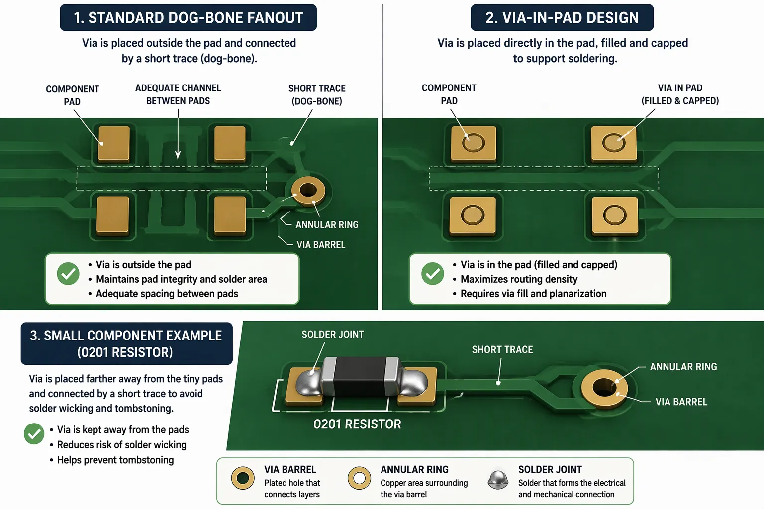
The previous cases show where a via belongs inside the pad. The reverse question deserves equal weight. Every via you move into a pad adds fabrication steps, and some layouts gain nothing from the move. Three situations call for a simpler structure.
Adequate Breakout Space
Standard dog-bone fanout remains the cheapest and fastest option when the pad has room beside it. A short trace leaves the pad, ends at a via, and the via drops to the target layer. The fabricator drills, plates, and tents that via with no fill step and no planarization. You save cost and lead time on every hole.
Check your pad geometry before you commit to a via in pad. Measure the channel between adjacent pads. Confirm that a trace plus a via fits inside that channel at your chosen line width and annular ring. If the answer is yes, keep the via outside the pad. A via-in-pad design only earns its cost when the breakout path disappears.
This check also protects assembly. A via outside the pad cannot wick solder from the joint. The joint forms on a solid land with no barrel underneath. You get a predictable reflow result with no fill inspection and no cap flatness concern.
Small Chip Components
Small chip parts punish a via placed on or beside their pads. Consider an 0201 or 0402 resistor. The pad is tiny, and the part sits on two small lands. A via near one pad changes how solder wets on that side. Paste wicks into the barrel, the joint starves, and the part tilts during reflow. Tombstoning follows.
The risk grows because these parts have little mass. A small imbalance in wetting force lifts one end. The part stands on edge, and the assembly fails inspection. Rework on an 0201 part is slow and risky.
Keep via in pads away from small chip-component lands. Route the connection to a via placed farther out, even if that costs a little routing space. Reserve the in-pad structure for the packages that truly need it, such as fine-pitch BGAs and thermal pads. A discrete part rarely justifies the added process.
Non-Soldered or Tented Vias
Many vias never meet solder paste. They sit outside pads, carry signals between layers, and receive a solder mask tent or a simple plug. These holes need sealing against the environment, not a solderable surface.
Full VIPPO treatment on such a hole wastes money. The fabricator adds via filling, planarization, and copper cap plating to a via that no paste will touch. You pay for steps that deliver no assembly benefit. Lead time stretches for the same reason.
Match the closure to the function. A tented via suits an ordinary signal hole. A plugged via suits a hole that needs partial sealing. Save the full fill and cap stack for pads that carry paste. This selective approach keeps pcb via filling costs where they belong.
The same logic applies across the board. Review every via-in-pad location and ask one question: does this hole sit under a solder joint? If not, downgrade it. A disciplined review of your via-in-pad designs often removes half the special callouts before release.
These three cases share a common signal. The pad has room, the part is too small, or the hole never meets paste. Any one of them points you toward a simpler via structure. Apply the test during layout, and your via-in-pad design stays lean and cost-effective.
Via in Pad PCB Design Guidelines
Via Size and Annular Ring
Start with the drill size and the annular ring. A small drill leaves more copper around the hole, and that copper supports a reliable copper cap. Ask your fabricator for the smallest drill they can fill cleanly. Fill material must reach the barrel bottom, and a narrow hole makes that job harder.
Keep the annular ring wide enough to hold the cap. A thin ring gives copper cap plating little to bond to, and the cap can separate during thermal cycling. Request the fabricator’s minimum ring for a capped via in pad. Apply that rule only to the pads that need it.
Solder Mask and Cap Coverage
Solder mask must not overlap the copper cap. A mask ledge over the cap lifts the stencil and starves the joint. Define the mask opening slightly larger than the cap, and confirm the expansion with your fabricator.
Cap coverage drives joint quality. The copper cap should span the full barrel and blend into the pad. Designing for via-in-pad means you treat the cap as part of the land pattern, not as an afterthought. Check every via in pads location against this rule before release.
Fab File Callouts and Selectivity
Selectivity is your main cost lever. Specify filled and capped vias (IPC-4761 Type VII) only on pads that carry paste. Full-board treatment adds cost and lead time for no gain.
Your fab notes must name each via that needs via filling, planarization, and copper capping. List the exact layer pairs, plus the drill and stackup notes. A vague “fill vias” note invites a dimpled pad. Clear callouts protect both via-in-pad filling quality and your yield.
Good pcb via-in-pad design also means matching the structure to the pad. Run a via in pad pcb design review to confirm each callout. A disciplined via-in-pad design review catches errors early. Apply via filling only where solder meets the hole. This via in-pad design habit keeps pcb via filling costs controlled. Document the copper cap thickness and diameter in the same note. That step makes your via-in-pad intent unambiguous.
Common Defects and Inspection
Voids, Dimpling, and Concavity
Industry data from IPC HDPUG and SMTA shows that via-in-pad structures carry real reliability challenges. The defects cluster around the fill and the cap, not around the drill itself. You can trace most field failures back to an incomplete barrel or an uneven surface.
Air pockets form when material fails to reach the barrel bottom. That trapped air expands during reflow and pushes through the joint. Solder balling follows the same path. A via filled but not capped properly, or tented on both sides without filling, gives that air a place to hide. Dimpling and concavity create a second problem. A dish in the pad holds flux and starves the joint of paste. Both defects pass a casual visual check, and both surface later as weak connections.
Solder Wicking and Head-in-Pillow
Solder wicking starts at the barrel opening. Paste flows into an open hole and leaves the joint short of material. The joint looks formed on inspection, yet it carries less solder than the design intends. A flat copper cap blocks that path and keeps the paste on the land.
Head-in-pillow is the harder failure. The solder ball sits on top of the paste without full coalescence, and the joint looks connected under standard inspection. The connection opens under thermal cycling or mechanical shock. This defect appears most often where a via in pad sits under a BGA ball and the cap surface is not flat. Proper via filling and planarization remove the gap that causes it.
Inspection Methods
X-ray inspection reveals voids inside the barrel and under the joint. You see the fill completeness without cutting the board. Cross-sectioning gives the definitive answer. A cut through the via shows fill material, copper cap thickness, and any gap between them. Reserve cross-sections for first-article qualification and failure analysis, since the cut destroys the sample.
Visual checks catch cap flatness and surface condition. Look for dimples, exposed resin, and mask encroachment on the cap. Pair that check with your fabricator’s inspection data. Ask for fill completeness results during via-in-pad design review, and confirm the pcb via filling records before you approve the lot. A disciplined inspection plan protects your via in-pad design from defects that only appear after assembly.
Cost Trade-Offs in Via in-Pad Design
What Drives the Added Cost
Every filled and capped via adds process steps that an ordinary tented via skips. The fabricator drills, fills the barrel, cures the material, planarizes the surface, and plates the copper cap. Each step needs its own setup, its own inspection, and its own queue time. That stack of steps explains most of the price difference.
Selective specification is your main cost lever. Full-board VIPPO treatment adds cost and lead time across every hole on the panel. A targeted callout limits the premium to the pads that carry paste. Review your via-in-pad designs with that discipline, and the premium stays small relative to the routing or thermal benefit you gain.
Balancing Density Against Budget
Density and budget pull in opposite directions, and neither wins by default. A dense board with no breakout room forces the decision. A board with spare routing area gives you a choice, and the cheaper structure usually serves you well there.
Weigh the trade-off honestly. A simpler via structure fits best when the pad has room beside it, when the part is a small chip component, or when the hole never meets solder. Reserve the full fill and cap stack for fine-pitch packages and thermal pads. This balance keeps pcb via-in-pad design affordable without sacrificing the joints that need protection.
Questions for Your Fabricator
Ask early, before layout freezes. Fill material, cap plating, and inspection capability vary between shops, and each answer shapes your design rules. A late question forces a redesign, and a redesign costs more than any via treatment.
Bring these questions to your first fabrication review:
Which fill material do you recommend for my drill sizes, and how do you verify a complete fill?
What copper cap plating thickness and flatness tolerance can you hold on a capped via in pad?
Which inspection methods do you run on via filling, and can you share the records?
What is the lead-time impact of selective versus full-board copper capping?
Clear answers let you finalize the via-in-pad design with confidence. They also give you a documented basis for the cost you accept.
Match the via structure to the pad, the pitch, the thermal load, and the budget. Do not default to the most complex option. Filled and capped vias earn their place under fine-pitch BGA and CSP packages, exposed thermal pads, and dense HDI routing. Skip them when breakout space exists, when small chip components sit nearby, and when a via never meets solder. Your pcb via-in-pad design succeeds through discipline, not through blanket rules. Confirm the IPC-4761 type in your fab notes, specify VIPPO only where paste meets the pad, and verify fill and cap quality with inspection. That checklist keeps every via in pad decision defensible, and it keeps your via-in-pad design affordable. Apply the same test to each via in-pad design callout, and your via-in-pad results will hold up in assembly.
FAQ
Does every via under a pad need filling and capping?
No. Reserve the full stack for pads that carry solder paste. A via that sits outside a land pattern and only needs sealing can stay tented or plugged. Blanket treatment raises cost and lead time with no assembly gain. Review each location and ask whether paste meets the hole.
Can I fill a via without capping it?
You can, but expect risk. Filling alone leaves a dimple or a soft resin surface, and trapped air can still expand during reflow. A copper cap restores a flat, solderable land. Use filled-only structures where the hole needs sealing but never meets solder.
How do I specify this correctly in my fab notes?
Name IPC-4761 Type VII, list the exact layer pairs, and state the copper cap thickness and diameter. A vague “fill vias” note invites a dimpled pad. Clear callouts protect both via filling quality and your yield. Confirm the requirement with your fabricator before release.
What drill size works best for a capped via in pad?
Ask your fabricator for the smallest drill they can fill cleanly. A narrow barrel makes a complete fill harder, and a thin annular ring gives the cap little to bond to. Match the drill and ring to their DFM limits, and apply that rule only where needed.
Do thermal pads need the same treatment as BGA pads?
Yes, for the same reason. An exposed thermal pad needs a flat, solderable surface, and open vias drain paste away during reflow. A solid fill also conducts heat better than an open barrel. Follow the IC datasheet for via count, drill size, and placement.
How do I verify fill and cap quality?
Start with X-ray to check fill completeness and voids without cutting the board. Cross-section for first-article qualification and failure analysis, since the cut destroys the sample. Add a visual check for dimples, exposed resin, and mask encroachment on the cap.
Where does via-in-pad design cost the most?
The added steps drive the premium: fill, cure, planarization, and copper cap plating, each with setup and inspection time. Selective specification is your main lever. A targeted callout limits the cost to pads that carry paste, and that discipline keeps via-in-pad design affordable.
When should I skip the in-pad structure entirely?
Skip it when the pad has room for standard dog-bone fanout, when a small chip component sits nearby, or when the hole never meets solder. Small parts like 0201 and 0402 tilt easily when one pad wicks paste. A simpler structure serves those cases better.