Your converter works fine on the bench. Then it gets to the EMC lab, and the scan fails. Or worse, it ships and blocks a nearby wireless link.
You can’t treat electromagnetic interference as a final checkbox. In ac-dc conversion, EMI suppression protects three things at once: regulatory compliance, product safety, and long-term system reliability. Electromagnetic compatibility failures also show up late, when a redesign costs the most.
Start with the physics. Find the noise source, trace the coupling path, then choose the filter. This guide is for hardware engineers and product teams who balance board-level design against manufacturing trade-offs every day.
Puntos Clave
Find the noise source and coupling path first. Then choose the right filter.
Differential mode noise needs an LC filter. Common mode noise needs a choke and Y capacitor.
Place input filters at the connector. Keep the Y capacitor return short to chassis.
Damp every LC stage to prevent ringing and keep the input stable.
Run bench pre-compliance tests early to catch emissions before the lab.
Noise Sources in AC-DC Conversion
The Switching Efficiency Trade-Off
Every ac-dc conversion stage makes a trade between efficiency and noise. You raise the switching frequency to make the transformer smaller and cut core losses. But that same fast edge creates steep voltage and current changes. Fast edges mean high dv/dt and di/dt, and those changes feed both conducted and radiated emissions.
You face a real tension here. A higher switching frequency improves power density in switch-mode power supplies, yet it pushes harmonic energy into frequency bands where your filter works less well. Slower edges soften the emi spectrum, but they burn more power in the switch. You should treat this as a variable de diseño, not a fixed setting. Choose the switching frequency and gate drive together, then check the resulting spectrum early.
Reading Noise with Fourier Analysis
A switching waveform is a periodic pulse train. Fourier analysis breaks that train into a fundamental and its harmonics. The harmonic amplitudes fall with frequency, and the envelope slope depends on the rise and fall times. You can use this to predict where the worst emissions will land before you build the board.
Notch frequencies in the spectrum come from the Fourier transform of the pulse-coded signal. One study worked out these notch equations for the pulse train alone, not the full converter. Simulated and measured notch frequencies matched the derived equations closely, and the authors left a full-converter derivation for future work.
The theoretical derivation of notch frequencies is presented, where the derived equations correspond to the Fourier transform of pulse-coded signals rather than the full converter system. Simulated and experimental notch frequencies closely match the derived theoretical equations, while derivation for the complete converter is deferred to future work.
Use this result with care. The pulse-train model gives you a useful first estimate for noise reduction planning in ac/dc converters. It does not capture every resonance in switched-mode power supplies, so confirm the prediction en la banca.
Main Coupling Mechanisms for EMI
Noise needs a path to become a problem. You can split the main coupling mechanisms for emi into two families. Each family acts in its own way, and each one needs a different fix.
Conductive and Radiative Paths
Conductive coupling needs direct contact. The source and the receptor share a wire, cable, Traza de PCB, or metal enclosure. Noise then moves along that conductor as common-mode or differential-mode current. Radiated coupling works in another way. The source and the receptor act like radio antennas. The source sends out an electromagnetic wave through open space, and the victim picks it up.
Camino de acoplamiento | Mecanismo | Caracteristicas claves |
|---|---|---|
Conductivo | Direct-contact path between source and receptor | Formed via transmission line, wire, cable, PCB trace, or metal enclosure; noise appears as common-mode or differential-mode on conductors |
Irradiado | Source and receptor act as radio antennas | Source emits an electromagnetic wave that propagates through open space and is picked up by the victim |
Inductive coupling, both capacitive and magnetic, also exists. Treat it as rare next to the conductive and radiated paths. When you debug a failing board, check radiation, conduction, or inductive or capacitive coupling in that order. The first two explain most failures.
Why Layout Shapes Coupling
Layout decides how strong each emi coupling mechanism becomes. A technical seminar used a real measured DC/DC converter to show this. Different Diseños de PCB changed the converter’s EMI signature directly. Passive component placement and selection changed EMC performance too. The same seminar presented filter strategies to meet CISPR32 Class B limits from 150 kHz to 1 GHz. That range shows layout-driven coupling must be managed alongside filtering.
Component proximity matters inside the filter itself:
Magnetic near-field coupling between PFC and CM chokes can degrade EMI filter insertion loss.
Layout, shielding, and CM choke design reduce that magnetic near-field coupling and suppress noise.
Coupling between two shunt capacitors changes filter behavior; negative mutual coupling can offset capacitor ESL.
In a CLC filter, balancing parasitic inductive and capacitive coupling between capacitors optimizes performance.
In a two-stage filter, a series inductor integration method exploits near-field coupling to improve low-frequency DM performance.
Good layout lowers emissions before any filter part is added. Fix the geometry first, then tune the filter.
Differential Mode vs. Common Mode Noise
Defining DM and CM Noise
You can’t fix noise until you know which mode carries it. The two modes differ in direction, path, and cure.
Common mode means signals or noise that flow the same way in a pair of lines; differential (normal) mode means signals or noise that flow in opposite directions in a pair of lines.
Differential mode noise goes out on one conductor and comes back on its return path. Common mode noise flows the same way on both lines and returns through ground or the chassis. That difference decides which filter you pick.
Aspecto | Differential Mode Noise | Ruido de modo común |
|---|---|---|
Definición | Noise sent through two conductors, one outbound and one return path | Noise current that enters no matter the outbound/return paths and flows the same way through two conductors |
Dirección actual | Opposite directions (currents cancel each other); also called normal mode | Same direction through both conductors |
Propagación | Stays within the power/signal line pair | Spreads over a wide area, though at low voltage levels |
Origen típico | Power supply and signal currents | Radiated noise leaking through metal casing or floor into other equipment |
Supresión | Cut by LC filters (inductor + capacitor) | LC filters don’t work; needs a common mode filter plus a capacitor at the input section |
An LC filter alone will not stop common mode emi. You need a common mode choke plus a capacitor at the input.
Measuring Noise with a LISN
A line impedance stabilisation network gives you a steady reference for ac/dc converter noise measurements. It shows a set impedance to the converter and isolates the mains. The network outputs two voltages, one on the phase line (Vp) and one on the neutral line (Vn). These relate to the mode currents by Vp = 50(ICM + IDM) and Vn = 50(ICM − IDM), with the 50 in ohms. Add the two outputs and the differential term cancels, leaving twice the common mode voltage. Subtract them and the common mode term cancels, leaving twice the differential mode voltage. Do this before measurement, because the analyzer loses phase information.
A practical sequence helps:
Remember that a LISN measures the sum of both modes and can’t separate them alone.
Clamp an RF current probe around line and neutral together to read common mode current.
Route the two wires in opposite directions through the probe to read differential mode current; the reading is 6 dB high.
Stay below the probe’s maximum current rating.
Compare both readings to see which mode dominates, then size the filter.
This step tells you whether to add DM inductance or X-capacitors. It also shows when conducted emissions come from the common mode path instead.
Selecting EMI Filters for DC/DC Inputs
When you pick emi filters for a DC/DC input, first ask what corner frequency you need. Set the LC corner to about one tenth of the switching frequency. A 1 MHz converter then needs a 100 kHz corner. With that gap, an ideal second-order low-pass emi filter gives about 40 dB of attenuation at the fundamental. Real boards give less, often around 30 dB, because capacitor ESL and trace inductance flatten the curve.
Parámetro | Objetivo | Nota práctica |
|---|---|---|
Frecuencia de corte | About 1/10 of switching frequency | Ideal attenuation near 40 dB at the fundamental |
Attenuation slope | 40 dB/decade ideal | Parasitics reduce the real slope |
Inductor value | 0.47 µH to 22 µH | Lower inductance cuts DCR and size |
1 µF a 100 µF | Check voltage rating and temperature drift | |
Damping Q | 0.5 a 0.8 | Add a damping capacitor of 3–4× the input capacitor |
L-C Filter Basics and Voltage Drop
A single LC low-pass stage is the simplest choice. A π-filter or a multi-stage network fits tighter limits or a source impedance that swings a lot. More capacitor stages improve high-frequency attenuation, but they raise inrush current and change the damping. Check stability again after you add each stage.
Watch the DC voltage drop across the inductor. DCR eats headroom, and a part rated for peak current may still saturate on a hot-plug event. Size the inductor for peak current, not average current. Keep the high di/dt loop short: place the inductor close to the converter input pins and return the current on a tight path.
Damping for Stability and CM Reduction
An undamped filter rings. The output impedance of the filter must stay well below the converter input impedance across the control-loop bandwidth. This is Middlebrook’s criterion, and ignoring it causes deep voltage dips, long overshoots, and input oscillation. You can check and pick emi filters with this rule before you touch a soldering iron.
Several damping options exist:
High-loss magnetic materials (Micrometals Mix-41, 44, and 73) damp filter resonances while passing fundamental current.
Damper circuits hold the peak at the cut-off frequency below 2–3 dB, which stops noise amplification in tests such as MIL-STD-461F/G CS101.
RC snubbers and resistive damping in filter capacitors steady the response.
Active damping is another choice when passive parts cost too much board space.
Use frequency response analysis to check damping, not time-domain testing alone. One trade-off needs attention: raising feedback loop gain improves noise reduction and filtering out emi, yet it can cut phase margin unless you compensate properly. For common mode, add a choke and a Y capacitor at the input; an LC stage alone will not stop it. These types of emi filters work together, and the right mix keeps emissions under the limit.
AC/DC Front-End Design for Low EMI
Rectification, Bulk Capacitors, and Inrush Limiting
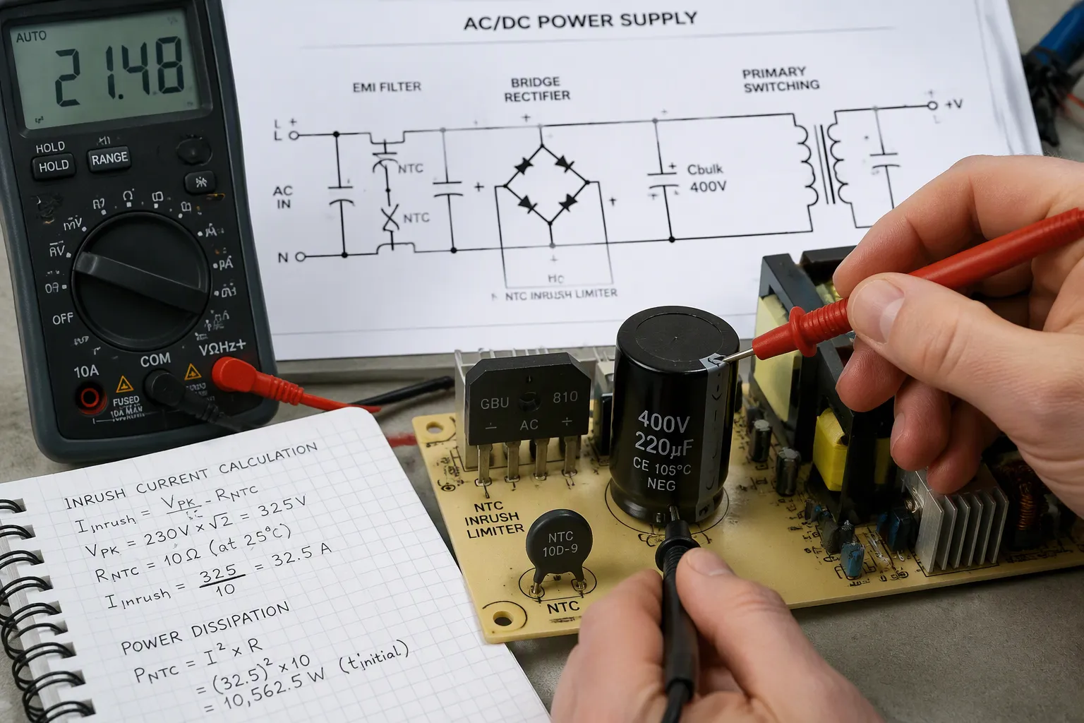
The front end sets the noise level for everything after it. Start with the bulk condensador. An uncharged electrolytic acts like a DC short when you power up. That short pulls a big inrush current, and the surge puts stress on rectifiers, fuses, connectors, and the capacitor itself. Size your inrush limiter for the stored energy and how often it repeats, not just the first plug-in.
Capacitor ESR changes more than ripple. Very low ESR can raise rectifier peak currents, so balance the part choice with diseño and a small series resistance instead of trusting the capacitor alone. When you swap a part, check ESR versus frequency and the ripple derating. Ripple current rating and ESR decide if the part survives, not capacitance and voltage alone.
Parameter / Choice | Effect on Ripple | Effect on Inrush / Rectifier Stress | Nota de diseño |
|---|---|---|---|
Capacitor ESR (too low) | Alters output ripple; interacts with ESL for hum/noise coupling | Very low ESR can increase rectifier peak currents | Balance via layout and optional small series resistance |
Capacitor ESR (different from original) | Changes output ripple and control-loop stability | Alters inrush behavior | Verify ESR vs frequency and ripple derating |
Clasificación de corriente de Ripple | Lower-rated substitute may run hotter and age faster | - | Ripple current and ESR determine survivability |
Capacitancia volumétrica | - | Uncharged electrolytic looks like a DC short at power-up | Use NTC, active limiter, or pre-charge resistor/relay |
Rectifier / return node placement | Placing the capacitor close to the rectifier reduces ripple coupling | - | Star grounding and RC/LC filtering help sensitive rails |
Paralleling capacitors | Increases ripple capability and lowers effective ESR | - | Symmetric copper routing and matched loop areas share current evenly |
Place the bulk capacitor close to the rectifier and the return node. Star grounding and RC or LC filtering on sensitive rails cut hum and noise coupling. Paralleling capacitors raises ripple capability and lowers effective ESR, as long as you route copper evenly and match loop areas so current shares equally.
For inrush, an NTC thermistor is cheap and simple, but it runs hot and wastes power after startup. Active limiting costs more and needs control logic, but it removes the steady-state loss. Weigh thermal headroom against bill-of-materials cost and assembly complexity before you decide.
PFC, Y Capacitors, and CM Chokes
A PFC stage adds its own switching noise on top of the main converter. Its switching frequency and harmonics interact with your input filter, so treat the PFC and the filter as one design problem. Check the filter corner against the PFC switching frequency, then confirm attenuation on the bench.
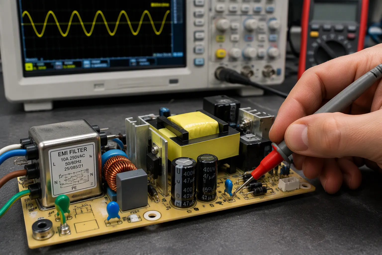
Safety capacitors sit in the EMI filter at the front end of the supply, often beside ferrite chokes on the input cable and common-mode or differential-mode chokes in the filtering stages. Class Y capacitors handle common-mode noise by giving a shared shunt point to earth. For an AC input to a DC supply, one Y capacitor connects line to earth and one connects neutral to earth.
Y-capacitors are designed to filter out common-mode noise and are connected between line and chassis. AC front-end products use an integral input filter comprising a common-mode choke together with Y-capacitors and X-capacitors.
Componente
Placement (Connection)
Role in EMI Filtering
Y capacitors (CY)
Line-to-Earth and Neutral-to-Earth
Filter common-mode noise
Common mode chokes (L1, L2)
In series on Line and Neutral
Provide inductance for common-mode filtering
X capacitors (CX)
Línea a neutro
Filter differential-mode noise
Place the CM choke before the Y capacitors in the current path, and keep the Y capacitor return short and direct to chassis. Long return traces add inductance and spoil the shunt. This setup is the backbone of low-emi design in switched-mode ac/dc supplies, and it matters most when you pick emi filters for tight limits. Good conducted emi performance in ac/dc converters depends on this front-end geometry as much as on part values. Treat ac-dc conversion as a chain: rectifier, bulk stage, PFC, then filters. Each link shapes the emissions you must suppress.
Topology and Transformer Choices
Flyback vs. LLC Resonant Trade-Offs
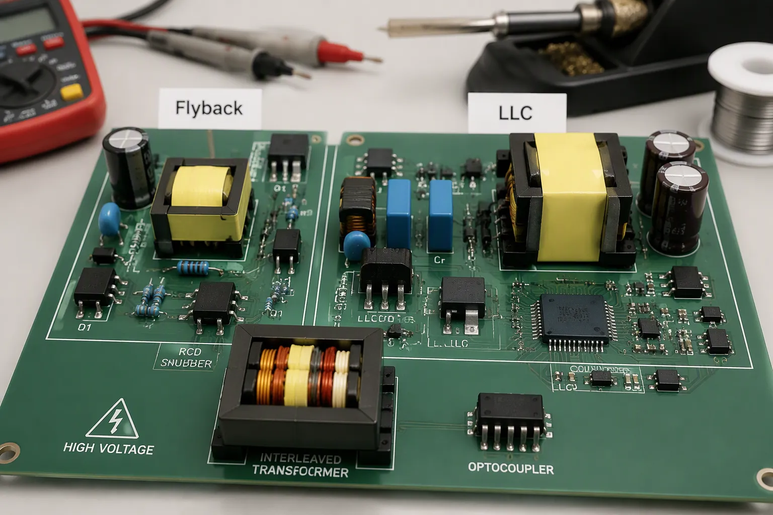
The topology you pick sets your noise level before you even choose a filter part. A flyback is part of the PWM hard-switching family. The transistor turns on while a large voltage is still across it. Parasitic capacitance charges up to that voltage and then dumps its energy through the transistor at turn-on. That energy comes out as heat and as emi.
An LLC resonant converter works in a different way. Its resonant tank lines up the turn-on with the natural voltage and current waveforms, so the switch sees zero voltage (ZVS). Soft switching cuts the capacitive dump loss. The result is better electromagnetic compatibility at high power levels, where a hard-switched flyback has a hard time.
Atributo | Volar de vuelta | LLC Resonante |
|---|---|---|
Modo de conmutación | Hard-switching under applied voltage | Soft-switching via resonant tank (ZVS) |
Turn-on loss | Capacitive energy dumped as heat and emi | Switching synced to natural waveforms |
EMI implication | Worse at high frequency and high voltage | Reduced loss, improved compatibility |
Compromiso de diseño | Simpler regulation | Better emi, more complex regulation |
You pay for the LLC gain with more complex control. Output regulation usually needs frequency modulation while the design holds ZVS. Choose the flyback for low power and simple control. Choose the LLC when efficiency and emissions both matter at higher power.
Transformer Design and Optocoupler Feedback
The transformer acts like an antenna as much as a magnetic part. How you arrange the windings in the window directly affects leakage inductance and parasitic capacitance, and both of these shape interferencia electromagnetica and efficiency. Tight layering keeps leakage low, which lowers the energy your snubber or clamp must absorb. Interleaving also tightens coupling, but it can raise capacitance.
Interwinding capacitance couples common-mode noise across the isolation barrier. High capacitance hurts common-mode performance and puts more load on your emi filters. A sandwich structure (primary–secondary–primary) reduces leakage, though it makes insulation harder. Shield windings and common mode chokes often become necessary to meet conducted and radiated limits.
Note: choose wire diameter on purpose. A smaller diameter lowers parasitic capacitance and skin effect, but it costs you higher current density.
The optocoupler feedback loop closes across that same barrier. Keep the optocoupler and its compensation network away from the switching node, and route the feedback trace clear of the transformer gap. Noise that couples into the feedback path shows up as jitter, and jitter spreads the emi spectrum in ways your filter was not tuned for. In ac-dc conversion, treat the transformer, the barrier, and the feedback loop as one layout problem.
EMC and EMI Design Strategies for Layout
Filter Placement and High-Frequency Current Paths
Bueno EMC and EMI design strategies begin with the return path. High-frequency current takes the path of least impedance, not the path you drew on the schematic. Give that current a solid ground plane, and it stays under the trace. Avoid ground splits under high-frequency traces. If you can’t avoid a split, bridge it with a stitching capacitor.
Put your input filters right at the connector, before noise spreads across the board. Keep switching regulators away from RF and analog sections. Keep high-frequency traces short, and use 45-degree or curved bends instead of 90-degree corners.
Estrategia de diseño | Práctica clave | Guías |
|---|---|---|
Plano de tierra sólido | Give a full layer to ground | Keeps return current under the trace |
Ground splits | Bridge gaps with stitching capacitors | Stitching capacitors across the gap |
Rastros de guardia | Flank sensitive lines, ground with vias | Vias spaced λ/20; crosstalk cut up to ~20 dB |
El desacoplamiento | Ceramic, low-ESL parts near power pins | 0.01–0.1 µF within 1–2 mm of pins |
Impedancia controlada | Match trace impedance to the system | 50 Ω for RF; FR-4 εr ≈ 4.2 |
When you pick EMI filters, check where the part sits, not just its values. A filter placed after a long trace picks up noise the trace already radiated. Test EMI filters on the real board, with the real return path. Filtering works only when the shunt capacitor has a short, direct path to ground.
Note: a decoupling capacitor placed far from the pin adds inductance and loses its effect at high frequency.
Creepage, Clearance, and IEC 62368 Spacing
Safety spacing limits your filter layout before electrical performance does. IEC 62368 sets the creepage and clearance you must hold across the isolation barrier. Y capacitors and common mode chokes sit right on that barrier. Their pads, traces, and slots must respect the required distance.
Measure creepage along the surface and clearance through air. A slot cut in the board raises creepage without adding height. Route the Y capacitor return straight to chassis, and keep other traces out of that zone. Check spacing again after you move a filter part for emissions. A layout that passes conducted limits can still fail a safety review.
Standards, Limits, and Pre-Compliance
CISPR 32 and EN 55032 Conducted and Radiated Limits
CISPR 32 and EN 55032 set the límites de emisión you must target for multimedia equipment. The standard covers both conducted and radiated emissions. Conducted limits apply from 9 kHz to 30 MHz for commercial equipment. Radiated limits run from 30 MHz upward. Your ac/dc front end sits on the mains, so it faces the full conducted limit. A DC/DC stage downstream sees a quieter source, yet its switching noise still feeds back through the converter. Treat the AC input as the strictest test point.
The LISN you use depends on the input type. Commercial AC mains need a 50 μH + 5 Ω || 50 Ω network, such as the Tekbox TBLC08. DC automotive work uses a 5 μH || 50 Ω network, such as the Tekbox TBOH01. Both give repeatable readings without an anechoic chamber.
Pre-Compliance Testing on the Bench
A bench workflow catches most problems before a lab visit. Follow these steps:
Identify the target standard, such as CISPR 32 or EN 55032.
Set up a spectrum analyzer with a pre-amplifier, a near-field probe set, and a LISN above a large ground plane.
Scan the board and cables with near-field probes to find hotspots.
Fix layout, shielding, or filtering, then re-test and compare.
Submit for certification once the margin looks safe.
Near-field probes work only at close range, a few centimeters. They give relative readings, so use them to locate sources, not to verify limits. A transient limiter is mandatory. AC turn-on transients can discharge up to ±325 V into mixer diodes rated for +20 dBm to +30 dBm RF. A limiter such as the Tekbox TBFL1 caps the output at +11 dBm under 5 W overloads.
Safety spacing under IEC 62368 constrains this work. Y capacitor pads and CM choke traces must hold the required creepage and clearance. Check spacing again after every filter change.
Thermal, Enclosure, and DFM Trade-Offs
Heat, Shielding, and Enclosure Effects
Heat and shielding both take up the same room inside a converter. Enclosure design, airflow, and where you put parts all affect how hot things get. You must check derating inside the final housing, not on an open bench. A part that stays cool on the bench can go over its rating once the case is closed.
Running nonstop or in harsh places needs extra margen térmico. That margin covers aging, dust buildup, and worst-case conditions. In small enclosures with limited airflow, even small efficiency losses can really cut usable power. Plan the thermal budget before you lock in the mechanical design.
Shielding changes emi in a direct way. A board-mounted module often sits near the input connections. Weak shielding lets radiated interference create conducted noise on those connections. Plastic module enclosures usually give no screening at all. An optional case kit can cut emissions that couple into the power supply conductors. Mix mechanical steps with electrical ones: shielding, careful layout, smaller loop areas, and solid ground planes, plus filtering, decoupling, damping, and bypassing. That mix helps you hit compliance targets such as EN 55022 Class B.
DFM Constraints on Filter Components
Your emi filters must make it through the linea de ensamblaje, not just the lab. Common mode chokes with fine wire break during handling. Large X capacitors need keep-out zones that fight your layout. Choose parts with standard footprints and reel packaging. Make sure the placement machine can handle the body size and weight.
Damping parts add cost and reflow steps. A damping capacitor of three to four times the input capacitor takes board area, and it may need a different dielectric. Check the solder profile for every added part. Ask your manufacturer about tombstoning risk on small capacitors near large thermal masses.
Test points and tuning pads help during pre-compliance work. They also add cost in volume. Decide early which pads stay and which ones you remove. Keep the filter layout stable across revisions, because a moved pad changes parasitic coupling and shifts your conducted results. Treat every filter change as a design change that needs a fresh bench scan.
Start with the noise type and the coupling path. Then pick and place the filters to match. That order saves you from guessing.
Three habits carry the most weight. Damp every LC stage so the input stays stable. Respect Y capacitor and IEC 62368 spacing limits, even after you move a part. Run bench pre-compliance early, so conducted emissions show up before the lab does.
Treat emi as an iterative board-level task, not a post-failure fix:
Set EMC targets during specification.
Test incrementally with a spectrum analyzer and near-field probes.
Tune only the failing frequencies.
Weigh manufacturing trade-offs early. Shielding fights heat dissipation, and fine-pitch structures raise cost. Bring your filter designer and PCB supplier into the ac-dc conversion review. Small requirement changes can force a full redesign.
Preguntas Frecuentes
Which noise mode should you chase first when a scan fails?
Separate the modes before you touch a part. Clamp an RF current probe around line and neutral together to read common mode current. Route the two wires in opposite directions through the probe to read differential mode. Compare both readings, then size your emi filter for the dominant mode.
Why does an LC stage fail to stop common mode noise?
Differential mode current flows out on one conductor and returns on the other. Common mode current flows the same way on both lines and returns through chassis or earth. An LC stage shunts the first path only. You need a common mode choke plus a Y capacitor at the input to suppress the second.
How do you keep a filter from ringing or oscillating?
Keep the filter output impedance well below the converter input impedance across the control-loop bandwidth. This is Middlebrook’s criterion. Add damping so the peak at the cut-off frequency stays low, and check the response with frequency response analysis rather than time-domain testing alone.
Where should the input filters sit on the board?
Place them at the connector, before noise spreads across the board. Keep the Y capacitor return short and direct to chassis. A shunt capacitor needs a tight path to ground, or trace inductance spoils its effect. Test the filters on the real board with the real return path.