Power design decides whether your product survives in the field. Battery life, heat limits, rail noise, and manufacturing cost all come back to a few board-level choices. You often lose energy in places engineers overlook: a leaking regulator, a peripheral left clocked, a wake source that fires too often.
The fix spans silicon features, board layout, and firmware. No single chip solves it. You need mcu control across all three layers.
A low-power microcontroller is a device specified for low current in sleep and active modes. Power management is the practice of gating, scaling, and sequencing supply and clocks to match real demand.
关键精华
Measure power use on your own board first. Find the part that uses the most power and fix that before anything else.
Use sleep modes and shut off peripherals you don’t need. Let the CPU sleep as much as it can to save power.
Choose the right regulator for each power rail. Use DC-DC converters for large voltage drops and LDOs for parts that are sensitive to noise.
Pick an MCU by looking at its measured current and wake-up time. Match its features to the duty cycle you actually use.
Design your board with good layout and heat control. Keep crystal traces short and use unbroken ground planes.
What Makes a Low-Power Microcontroller?
Defining Low-Power MCUs
A low-power microcontroller is built to use very little current in every state, not just when the CPU runs. The label alone does not mean much. You should judge a low-power MCU by what stays on in each mode and what it takes to leave that mode.
Sleep modes shape much of that behavior. A typical ladder looks like this:
Sleep: the CPU and most peripherals turn off, but registers and memory stay kept, and an external interrupt or watchdog reset wakes the device.
Idle: the CPU clock stops, but peripherals keep running, so the part still reacts to events.
Deep sleep: most internal circuits shut down, and only the watchdog and external-event detection stay active.
Some low-power microcontrollers add user-selectable regulator settings during sleep. Lower power settings mean longer wake-up times. Peripheral Module Disable lets you switch off unused blocks to save even more.
Key Characteristics to Evaluate
Compare low-power microcontrollers by measured current, not by mode names. Wearable timekeeping with an RTC running can sit near 0.3 µA, and some standby cases reach 0.1 µA. A SLEEP mode in a security device can also hold 0.1 µA, or 0.2 µA with the RTC active.
米制 | 它告诉你什么 |
|---|---|
有功功率 | Current per MHz while the CPU executes |
待机电流 | Leakage when nearly the whole device is off |
起床时间 | Clock settle and regulator ramp delay |
保留成本 | SRAM kept alive during sleep |
Energy per wake-up cycle matters as much as sleep current. Analog settling can take milliseconds. Leakage sets the floor on battery life, and it roughly doubles every 10°C rise, so check total system leakage at your temperature extremes. For a fair comparison across vendors, use ULPMark-CP for deep-sleep energy and ULPMark-PP for peripheral impact. Pick the low power MCU whose wake sources and latency fit your duty cycle.
Power Consumption Fundamentals
Dynamic vs. Static Power
Dynamic power is the energy used when signals switch. Each clock edge charges and discharges the capacitance in gates and wires. Dynamic power goes up with capacitance, with supply voltage squared, and with frequency. You control all three by setting clock rate, rail voltage, and how much of the chip stays active.
静功率 is the current that flows when nothing switches. It comes from leakage in every transistor on the die. This part of power use does not depend on your clock speed. It flows as long as the rail is up, so it sets the lowest standby current for any microcontroller.
Frequency, Voltage, and Leakage Scaling
Leakage scaling depends on the process and on the ratio of supply voltage to threshold voltage. Signal activity plays no part. Several factors set the amount:
Subthreshold leakage depends exponentially on gate-source voltage and threshold voltage.
Transistor width-to-length ratio and process parameters set the absolute level.
Raising threshold voltage or lowering supply voltage cuts leakage, but it costs switching speed.
Leakage goes up with temperature, so hot corners can dominate your worst-case budget.
In advanced nodes, leakage makes up about 40-60% of power loss. High-K gate dielectrics and body biasing help push it below 100 pA/µm.
Advanced nodes such as 22nm FD-SOI support subthreshold operation, but subthreshold operation makes the chip more sensitive to temperature changes, so performance should be checked from -40°C to 85°C.
For a low-power MCU, scale frequency first, then voltage. Check mcu power consumption at your real duty cycle, not at peak. Measure power draw in each sleep state on your own board. A low power MCU with good leakage numbers still wastes power if your firmware never lets it sleep.
Low-Power MCU Architecture
Sleep Modes, Clock Gating, and Power Domains
Sleep modes set the lowest point for your energy budget. Current draw usually drops a lot as you go down the ladder. Sleep is about 2–5 mA, stop is about 20–100 µA, and standby is about 1–5 µA. Your wake sources decide how often you go back up. GPIO edges, the RTC, an analog comparator, and an ADC threshold can all wake the chip. Pick the slowest trigger your application can handle.
Clock gating stops the clock to blocks that are idle, and power-domain partitioning cuts the supply from whole areas of the die. These chip-level domains match up with board rails. A domain you never use should get no voltage at all. That mapping is the core of microcontroller power management.
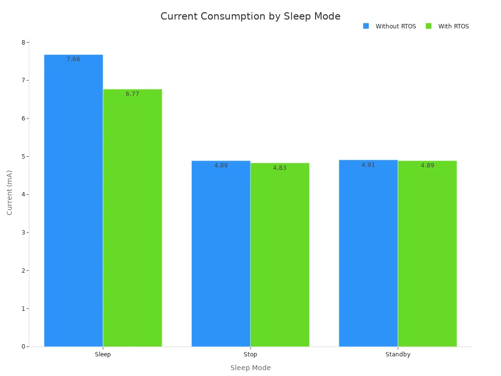
Firmware should lower frequency first, then voltage, when scaling. Frequency scaling is instant and safe. Voltage scaling needs a stable regulator and a settling delay. Use this order inside every low-power mcu architecture you build.
Timers, ADCs, and On-Chip DC-DC Converters
Low-power microcontroller architecture relies on peripherals that run without the CPU. A low-power microcontroller with a low-power timer can wake on a long interval and let the core stay in deep sleep. The ADC helps when it compares against a threshold in hardware. The core then wakes only on a real event. This cuts active time and improves mcu power consumption at the system level.
An on-chip DC-DC converter changes the trade-off. It keeps efficiency across a wide input range and lowers heat. A low-power MCU with an integrated converter often beats an LDO-based rail in deep sleep current. Check the converter quiescent current before you commit. A low power MCU is only as good as its supply.
Treat the MCU as the center of microcontroller power management. Gate each peripheral rail on demand. Measure sleep current in every mode on your own board. A low-power MCU architecture rewards this discipline. A low power MCU that never sleeps wastes its silicon. Deep sleep is a firmware decision, not a datasheet feature. Deep sleep current depends on what you leave enabled. Deep sleep only pays off when every unused block is off.
Why Power Matters for IoT and Battery Devices
Battery Life and Energy Budgeting
A battery-powered device depends on its 能源预算 to keep working. You begin with the milliamp-hours in the cell and split them across every task the product does. Sleep current, wake-up energy, radio bursts, and sensor settling all pull from the same pool. One load you overlook can take over the total.
Build the budget from measured numbers, not estimates. Profile the power draw of each state on your own board. Then multiply each state current by the time the device spends there. The sum shows you the real battery life. If the result falls short, find the largest term first. Most designs lose more energy to idle peripherals than to active computing.
热稳定性和可靠性考虑因素
Electrical resistance in semiconductors makes heat in proportion to current flow and switching frequency. Higher clock speeds and denser integration make this worse. Junction temperature is the parameter that matters. Silicon devices are usually rated for maximum junction temperatures of 85°C to 150°C depending on grade. Going past those limits speeds up aging through electromigration, thermal cycling stress, and metallization degradation.
Package thermal resistance, often 20°C/W to 60°C/W for QFN and BGA parts, creates a gradient between die and ambient. Localized hot spots at CPU cores, PLLs, and power management units can run 20–30°C above the average die temperature. Each 10°C rise in operating temperature can possibly cut the expected lifespan of the device in half, following the Arrhenius equation for failure rate acceleration.
You have several levers to 减少热量 and extend service life:
Select a part with lower thermal resistance in the same package.
Improve the heat sink or move to active cooling.
Reduce switching frequency to cut dynamic losses.
A temperature swing of 70 K derived from the load profile allows a maximum heat sink temperature of 55°C when the chip temperature limit is 125°C.
Check the power requirements of every rail against these limits. A conservative thermal design with margin beats a tight one when cost permits.
Power Management and Energy Efficiency in Practice
Firmware Techniques to Cut Active Time
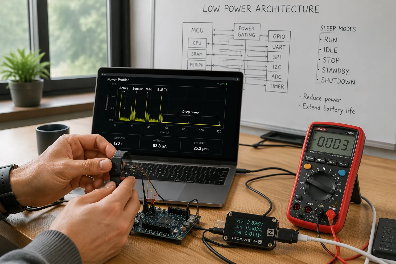
Time is your biggest lever. Cut the time spent actively processing and let the system sleep more, and the whole system’s power draw drops. The sleep current the MCU advertises sets the floor. How firmware schedules tasks sets the ceiling on what you really get.
A wearable sensor program showed this clearly. The main loop was busy-waiting on I2C transactions instead of entering WFI, the Cortex-M instruction that stops the CPU clock until the next interrupt. Every later fix — sensor timing, clock tree, eMMC clock rate — was limited by that one decision. Polling loops cost you 200 µA to 3 mA. Interrupt-driven wake removes that cost.
Firmware Technique | 典型节省 | 功夫 |
|---|---|---|
Correct sleep loop, no spin | 500 µA – 2 mA | 低 |
Radio duty cycling | 50–800 µA avg | 中 |
Peripheral power gating via load switch | 7–800 µA | 中 |
SPI pin state on sleep (drive low) | 10–30 µA | 低 |
Interrupt-driven wake, no polling | 200 µA – 3 mA | 中 |
SPIM DMA + PPI shortcut | 50–200 µA | 高 |
DC/DC regulator enable | 20–50 µA active | 低 |
Clock source selection | 0.1–0.9 µA | 低 |
On the nRF52840, System ON with the CPU off draws about 1.5 µA plus peripherals and wakes in about 6 µs. System OFF draws about 0.4 µA but wakes as a cold boot, costing roughly 20 ms and 6 mA·ms per event. At realistic event rates, System ON won.
Pick deep sleep states with care. Deep sleep only pays off when every unused block is off. Choose digital sensors that wake on interrupt or batch their data. Avoid sampling the ADC all the time, which forces the MCU to stay active. Use event-driven triggers so peripherals and displays turn on only when needed. These power optimization techniques raise energy efficiency without new hardware.
Peripheral and Rail Gating Strategies
Think of the microcontroller as a smart power control center. Build a power-control mechanism so modems, displays, ADCs, and sensors switch off when idle. Account for power-up time and inrush before you gate a rail. Some loads cannot handle a full power cycle.
Rail gating pays when two voltage domains give real savings. You accept an extra converter and level shifters in return. Prefer switching DC-DC converters over LDOs, because a linear regulator burns the voltage drop as heat. Turn off internal MCU modules when unused, and drive them dynamically in code.
Prioritize peripherals over MCU selection. If the board draws about 500 mA while the MCU uses about 10 mA, optimizing the part yields little. Gate the big loads instead. For harvesting designs, nanoamp-level quiescent current in the regulator keeps the rail alive between events. Measure every stage with a profiler rather than estimating. That discipline protects battery life and power efficiency across revisions.
Board-Level Power Design for Microcontrollers

LDO vs. DC-DC Trade-Offs
The regulator you pick sets your efficiency, heat, and noise before any firmware runs. Compare the two options on the points that matter for your rail.
维度 | DC-DC转换器 | LDO 稳压器 |
|---|---|---|
高效 | Usually 80–95% | Usually 50–70% |
发热 | 降低 | 更高 |
Output noise | Higher (switching ripple + EMI) | Very low, barely any ripple |
外部组件 | Several (inductor, capacitor, switching elements) | 少数 |
静态电流 | 有时更高 | 通常非常低 |
最佳使用 | High-current systems with a big voltage drop | RF, analog, and noise-sensitive rails |
LDO loss grows with the voltage drop and the load current. A 5V to 3.3V rail at 100mA wastes 0.17W, which is easy to handle. A 12V to 3.3V rail at 500mA wastes 4.35W, which is too much heat. Pick a DC-DC converter as the drop and current get bigger.
Noise decides the rest. Switching ripple hurts ADC accuracy, high-frequency harmonics lower RF sensitivity, and switching spikes cause audible hiss in audio paths. A common setup runs battery or 12V into a DC-DC bulk step-down, then an LDO for noise cleanup, then the RF, ADC, and sensor rails. A precision 24-bit ADC on a 5V to 3.3V rail needs an LDO, because 10–30mV of buck ripple would drown out microvolt signals. An automotive 12–14V to 5V rail at 1.5A needs a buck, because an LDO would waste about 13.5W. An IoT RF transceiver at 9V to 3.3V and 300mA works best with a hybrid: buck to 3.6V, then LDO to 3.3V, wasting only 0.09W.
Rail Sequencing, Decoupling, and Noise
Decoupling keeps the voltage steady when load transients hit. Place energy-storage capacitors as close as you can to the circuits that cause the transients. This local supply shrinks the current-loop area and lowers parasitic inductance.
请遵循以下放置规则:
Mount each capacitor next to its VDD–VSS pin pair and keep the loop small.
Pair a 0.1 µF high-frequency capacitor with a nearby 4.7 µF or 10 µF bulk capacitor.
Use one capacitor per power pin, and never share capacitors between distant pins.
Tie one terminal to the VDD trace and drop the other straight through a via into the ground plane.
Use continuous ground and power planes so return paths stay low-impedance. Add ferrite beads or small resistors on VDD lines to form RC or LC filters. In mixed-signal boards, join analog and digital grounds at a single point and filter AVDD separately.
Check brown-out and reset behavior early. A reset supervisor must hold the MCU in reset until the rail is stable, and GPIO lines that leave the board need series resistors and clamp diodes.
These steps protect mcu control during startup and keep microcontroller power management predictable across builds.
Layout, Thermal, and DFM Considerations
Crystal, Clock, and Ground Plane Layout
Put the crystal as close to the microcontroller as the package will let you. Short traces cut noise and keep the signal clean. Route those traces in a balanced way, because uneven lengths can make the oscillation unstable. Keep vias off the crystal traces, since extra inductance hurts timing accuracy. Use load capacitors with values that match the crystal spec, and connect them to a low-impedance ground.
Long traces add unwanted inductance and capacitance. They change the load the crystal sees and make the oscillator more open to EMI. Route crystal traces away from high-speed switching signals and power lines. Noise that couples in raises jitter, makes phase noise worse, and can even stop a reliable startup. Guard rings and local copper pours boost immunity, but too much copper near the pins adds stray capacitance. Balance shielding against loading, and follow the crystal maker’s advice on capacitor values, drive level, and startup margin.
Ground plane strategy backs all of this up. Use one continuous plane under the mcu, and keep return currents short. Filter the ADC reference on its own, because reference noise shows up directly in your readings.
Thermal Design and Manufacturing Trade-Offs
Heat shortens life. Junction temperature drives aging, and packages rated for 85°C to 150°C leave you little room at the top of the range. Package thermal resistance of 20°C/W to 60°C/W for QFN and BGA parts sets the gradient from die to ambient. Copper pours under the part and thermal vias to inner layers spread that heat. Check every rail against these limits before you lock the stackup.
DFM constraints shape the same choices. Thin traces save space but add resistance and heat. Via-in-pad boosts thermal performance and costs more to make. Panel use and layer count drive cost, so confirm your fab’s minimum drill, annular ring, and solder mask clearance early. A layout that ignores these rules comes back as a re-spin. Review thermal and DFM together, and the power design survives both the bench and the line.
选择合适的MCU
Criteria and Trade-Offs
Begin with current you actually measured, not the names of the modes. Divide active current by MHz so you can compare parts on equal footing. Look at sleep current, since it decides how long your battery lasts while idle. Then make sure flash and RAM can hold your firmware, security libraries, and OTA image.
标准 | 为何重要 | Typical low-power IoT range |
|---|---|---|
有功电流 | Controls energy during compute bursts | ~30–120 µA/MHz |
Sleep/standby current | Sets idle battery life | ~50 nA – 5 µA |
Flash | Holds firmware, security, OTA | 约 64 KB – 1 MB |
内存 | Buffers sensor data and crypto blocks | ~8 KB – 256 KB |
集成无线电 | Cuts external parts and leakage paths | BLE / Sub-GHz / Wi-Fi SoC |
Balance speed against battery life. A faster clock gets work done sooner, but it pulls more current at that moment. Short bursts followed by deep sleep usually keep total energy lowest. Also weigh cost against integration. A separate mcu plus an external radio lowers the unit price, but it adds board leakage and regulator losses. An integrated SoC makes layout and power integrity simpler, though the silicon costs more.
Popular MCU Families Compared
ARM Cortex-M parts, such as the STM32F0 and STM32F3, give you low-power modes and a strong ecosystem. The STM32F0 aims at saving energy, while the STM32F3 trades power for speed. Espressif ESP8266 and ESP32 include Wi-Fi, and the ESP32 adds Bluetooth. The ATmega328 stays cheap and simple to use, with solid community support.
The MSP430 earned its name through ultra-low-power operation. Newer ARM Cortex-M0 and STM32U0 families have mostly caught up. The MSP430 still holds a real edge with FRAM, which offers almost unlimited write endurance and very low write energy. That fits energy harvesting and constant logging. For most new designs, look at Cortex-M0 or STM32U0 first. Pick MSP430 when FRAM matters. Upgrade paths include TI MSPM0 or STM32U0.
Match your OS to your memory and power needs. FreeRTOS works on small parts, and Embedded Linux needs much more RAM and flash. Treat mcu/processing unit optimization as a whole-system job. The best energy-efficient mcu still wastes power if your firmware never sleeps. Compare low-power microcontrollers using your own duty cycle. A low-power microcontroller with great numbers can still lose to a low power mcu with better wake latency. Choose the low-power mcu whose wake sources fit your events. That choice beats any single spec sheet. A low power mcu that fits your workload wins.
Future Trends in MCU Power
Process Advances and Integrated Power Conversion
Chip makers keep making silicon process nodes smaller, and each step lowers the voltage a core needs to switch. That drop cuts dynamic power, but leakage becomes a bigger share of the total. Designers respond with body biasing, high-K dielectrics, and finer power-domain partitioning. Expect future parts to offer more domains, not fewer, so plan your rail budget with extra room.
Integration is the other big shift. Vendors now put buck converters and LDOs on the same die as the core. One recent 32-bit ARM Cortex-M0 part runs at 24 MHz from 1.8–3.3 V and draws 18 µA/MHz on CoreMark. Its deepsleep current sits at 340 nA with the RTC and 8 kB of SRAM kept alive. On-chip inductive buck converters, an LDO, and a 1 MHz low-power mode make that possible. You get better energy efficiency because the converter matches the core voltage instead of burning the difference as heat.
Energy Harvesting and Ultra-Low-Power Operation
Harvesting is moving from lab demos into smart tags and sensors. Dual-source designs now pair radio frequency with photovoltaic cells, so a tag keeps working when one source fades. A companion PMIC handles the harvesting front end. Vendors offer parts for photovoltaic, RF, vibration, thermal, and dual-source inputs, plus hybrid low-to-high power variants.
Treat the mcu as the supervisor of that harvested rail. A low-power mcu should wake on a comparator or timer, take one reading, and go back to deep sleep. The low power mcu in the table above keeps 8 kB of SRAM alive in deep sleep, so you avoid a cold boot on every event. That habit protects battery life in products that still carry a cell. Choose a low-power mcu with a wide supply range and a true 1 MHz mode. Then measure the quiescent current of every rail, because harvesting leaves no power to waste.
Measure power first. Then use architecture, firmware methods, board-level design, and smart MCU selection, in that order. Each layer builds on the numbers you gathered before it.
Good power design takes repeated passes. It covers silicon, board, and software. No single chip choice gives it to you, and no single pass finishes it. You improve mcu control as your measurements get better.
Start now. Profile the current design and find the biggest power user. Fix that first, then measure again. Keep DFM and manufacturing trade-offs in mind, and your microcontroller will hit its battery life goal.
常见问题解答
How do I measure real sleep current on my own board?
Measure at the rail, not at the bench supply. Cut the trace to the MCU and insert a current shunt or a jumper for a meter. Let the firmware enter each sleep mode and log the current for several minutes. Subtract regulator quiescent draw. Datasheet numbers rarely match your board.
When should I pick an LDO instead of a DC-DC converter?
Pick an LDO for noise-sensitive rails such as ADC references, RF front ends, and 模拟传感器. Pick a DC-DC converter when the voltage drop and load current are large. A hybrid works well: buck down close to the target, then LDO for cleanup. This keeps heat low and noise controlled.
Which wake source should I choose for a battery device?
Choose the slowest trigger your application can tolerate. A GPIO edge wakes fastest but fires often. An RTC alarm, analog comparator, or ADC threshold wakes less often and saves more power. Match the wake source to your real event rate, then measure the energy per wake cycle.
How do I judge a low-power claim on a datasheet?
Ignore mode names and compare measured current per MHz in active mode. Check standby current, wake-up latency, and SRAM retention cost. Run ULPMark-CP and ULPMark-PP numbers if the vendor publishes them. Then confirm the figures on your own board at your temperature extremes. A good MCU earns its rating in your circuit, not on paper.
Efficient power design rewards patience. Profile first, fix the largest consumer, and measure again. Each pass brings your product closer to its battery life target.