Two board-level choices decide if your industrial IoT product succeeds. The first is a careful radio duty cycle and sleep plan for low-power BLE communication. The second is interface design—antenna, power, and digital I/O—that holds up in harsh places.
The stakes are real. You need batteries that last for years and steady behavior in a crowded 2.4 GHz spectrum. You also need a design that builds cleanly at high volume. A careless ground plane or a noisy rail can wipe out your battery life gains before the first field unit ships.
This post gives you practical PCB and PCBA guidance: part selection, layout rules, and DFM trade-offs. You will not find general BLE theory here—only choices you can use on your next board.
Zvitsva Zvitsva
Pick a long advertising interval to save battery power.
Use sleep modes and group sensor readings together to lower power use.
Choose a BLE module that is already certified to avoid the cost of RF certification.
Put the antenna at the edge of the board, and keep the ground plane in one piece.
Check the sleep current on a real board to find hidden power drains.
Low-Power BLE Communication Strategies
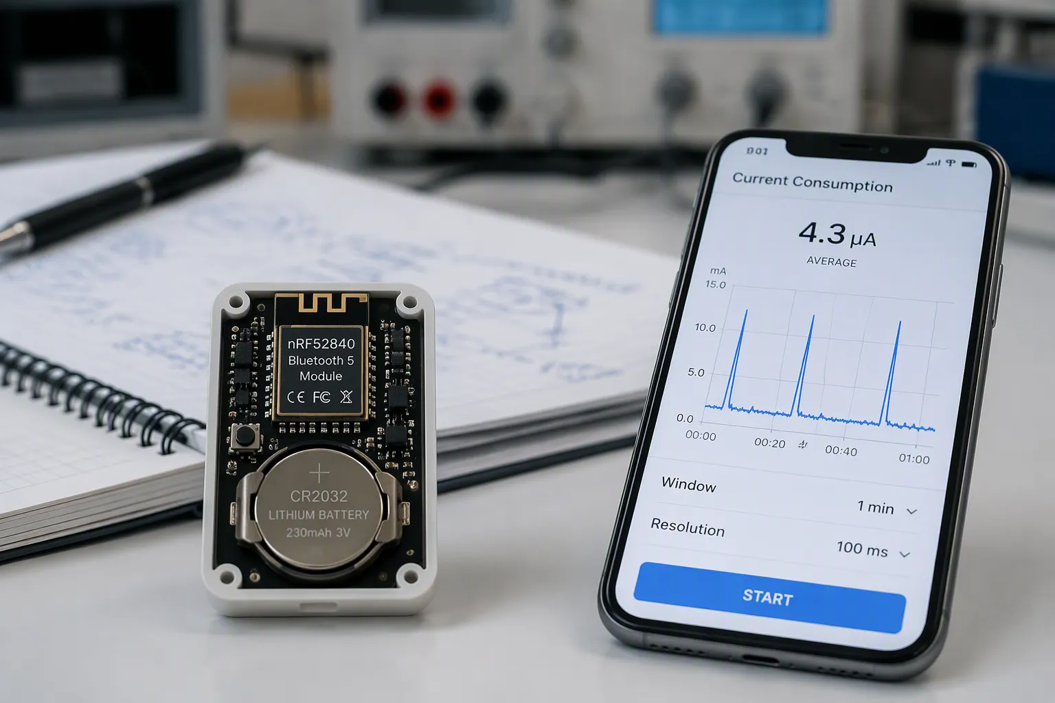
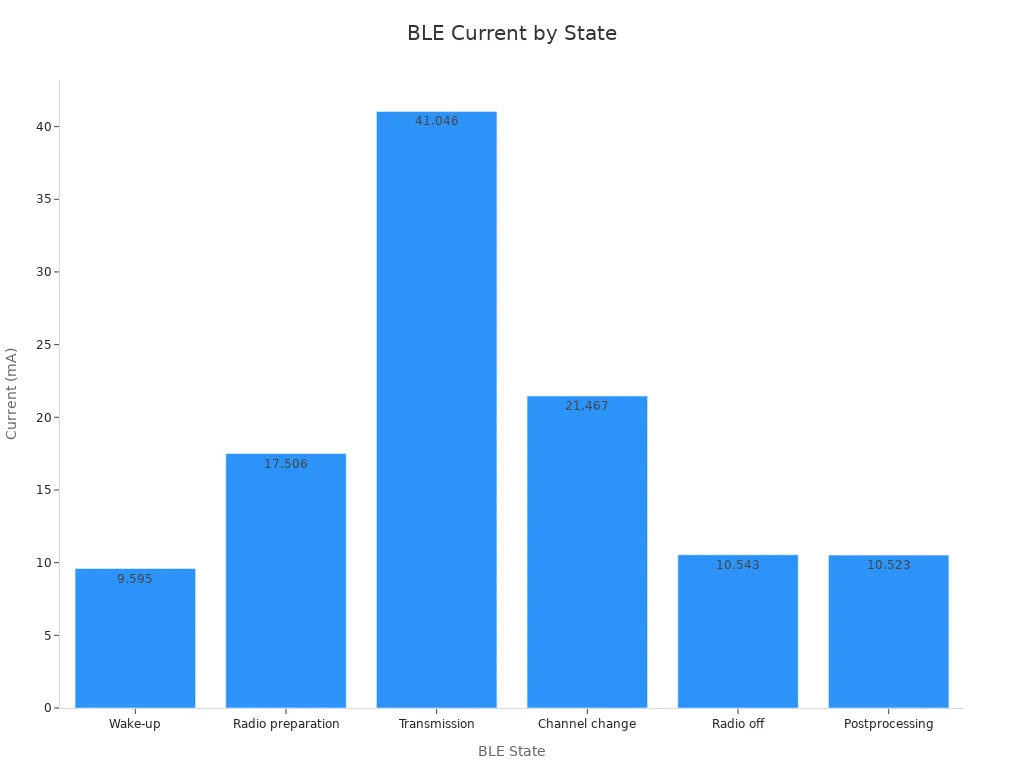
Bluetooth low energy keeps the radio off most of the time. The device wakes up, sends a short burst, and goes back to sleep. Your current budget comes straight from that duty cycle. A radio that pulls tens of milliamps for a few hundred microseconds still averages microamps if you schedule it well.
Advertising and Connection Parameters
Start with the advertising interval. The BLE specification measures it in 0.625 ms units, and connectionless advertising is allowed from 100 ms kusvika 10.24 s. Longer intervals cut average current a lot:
Advertising Interval | Average Current Consumption |
|---|---|
100 ms | ~81.0 µA |
1 s | ~9.4 µA |
10 s | ~2.3 µA |
The active advertising phase draws anenge 10.9 mA. At the shortest interval of 20 ms, total average current during advertising hits about 2.3 mA.
Connection parameters matter just as much. You can adjust the connection interval between 7.5 ms and 4 s. An adaptive connection interval lets you trade latency for current. Slave latency gives you another lever:
With a connection interval of 75 ms, changing the slave latency value to 5 can drop the average current consumption from 230 µA to 140 µA (a 40% saving).
A short interval with high latency gives you the best of both. The peripheral skips connection events when it has no data, yet it can transmit in the next event when data is ready. This is dynamic connection management in practice, and it is the core of low-power BLE communication.
Sleep Modes and Low Power Consumption
Sleep current sets your floor. A BLE SoC in deep sleep draws far less than in standby, so pick the lowest state you can and enter it right after activity. Firmware scheduling decides how often you wake. Waking up often adds setup overhead that dominates energy use. Batch samples per wake-up instead. One study buffered ECG samples in a sensor FIFO, woke the MCU on interrupt, read out over SPI, transmitted, and returned to system-off. Raising the FIFO threshold to its maximum cut MCU power to about 0.5 mW. Centralize power control in one firmware module so components request and release performance levels. This low-power architecture is what delivers low power consumption at the board level.
Payload Efficiency
Send fewer, larger packets. A larger ATT MTU raises throughput by up to about 15% and slightly lowers power because you need fewer transmissions. Data Length Extension shortens active transmit and receive time. Prefer notifications over indications:
Notifications are preferable to indications because indications demand a round-trip confirmation before another message can be sent.
Write Commands work the same way. They are asynchronous and can go back-to-back within one connection event. Write Requests are synchronous and usually allow one operation every one or two events. Avoiding round trips is the simplest route to better energy efficiency, and it keeps your BLE protocol stack work light.
BLE SoC and Module Selection
Your first choice is the radio itself. You can build around a separate SoC or use a module that is already certified. Each path changes how much RF layout work you do, how much certification you face, and your DFM risk.
Bluetooth Low Energy SoC vs. Module
A pre-certified module comes with the radio, crystal, and antenna already tuned and tested. You treat it as one component. A separate SoC puts the RF front end on your own board. You own the matching network, the antenna testing, and the FCC and CE filings.
The cost gap is large. A separate BLE design costs, covering development, manufacturing, RF certification, and testing, can range from $ 100,000 kuti $ 200,000. Pre-certified modules remove the time and cost of RF radio certification and can drop into a design in days to weeks.
Metric | Pre-certified BLE Module | Discrete SoC Design |
|---|---|---|
Certification ownership | Included (usually) | You own 100% |
Time to first working prototype | Mazuva-vhiki | mwedzi |
Failed FCC test penalty | Avoided (pre-certified) | $10K–$30K retesting fees + 6–12 weeks schedule slip |
RF layout, tuning, antenna characterization, FCC/CE certification | Not required (drop-in) | Bhajeti remwedzi 2–3 |
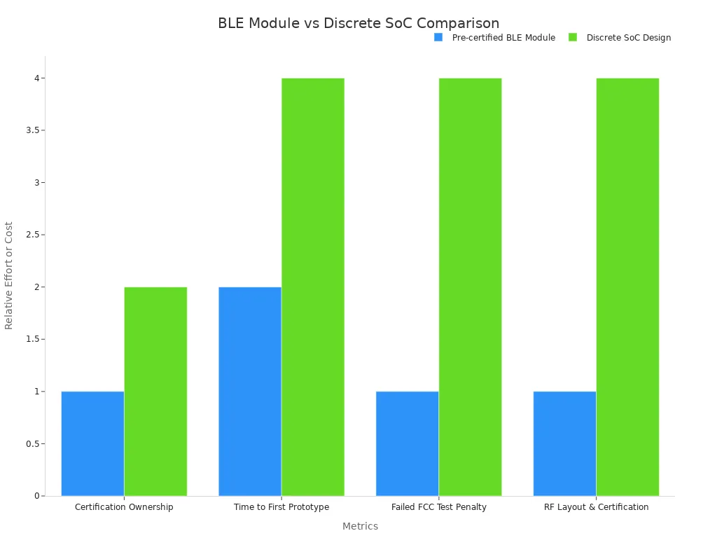
Pick the module when volume is moderate and schedule matters. Pick the separate SoC when unit cost rules at high volume and your team owns RF test equipment.
Makiyi Ekusarudza
Sleep current sets the floor for your battery life. A BLE module built on the EFR32BG21 SoC draws about 4.5µA in deep sleep, measured with the RTC active and memory kept. That number belongs in your power budget before you pick anything else.
Wake-up latency matters too. Vendors talk about fast wake-up and multi-level power-saving modes, yet many datasheets give no numeric latency. Ask for measured wake-up time, then check it on your own board.
Check the crystal requirements and the low-power modes the part offers. An external PA/LNA buys range at the cost of current. Your low-power architecture design must account for both.
Bluetooth Low Energy version support shapes industrial fit. Core 5.0 adds LE 2M and LE Coded PHY for longer range. Core 5.2 adds LE Power Control and Isochronous Channels. Core 5.3 adds LE Connection Sub-Rating for fast duty-cycle switching. Match the version to your sensor network, not to a datasheet headline.
RF Layout and Antenna Design
The antenna is the one part of your BLE design that firmware cannot fix. Where you place it and whether the ground plane stays unbroken decide your link budget before you tune anything.
Antenna Placement and RF Keep-Out
Put the antenna at a board edge, with the keep-out zone reaching past the board outline. Follow the module datasheet for exact keep-out sizes, because the feed area is very sensitive. If you break the keep-out, your link budget drops. Keep the ground plane fully unbroken under any 50-ohm RF trace that runs to the antenna connector. Avoid slots or voids from connector cutouts or via fields, since they cause impedance discontinuities. Do not route signal traces through the ground pour under the BLE module.
Stitch the RF ground with dense vias. Use 2–3 mm spacing around the antenna keep-out region and along the edges of the RF ground pour. Ground-via spacing should be at least λ/10, which at 2.4 GHz is about 6 mm.
Frequency (GHz) | Wavelength (cm) | Recommended via spacing (λ/10) |
|---|---|---|
2.4 | ~ 12.5 | ~ 6 mm |
2.5 | 12 | 6 mamirimita |
Matching Network and Clock Placement
Tune the matching network inside the final enclosure. The enclosure material strongly affects tuning, and metal is very harmful because it conducts. Even low-metal paint has a big impact. Nearby metal objects and PCBs cause currents, act like small radiators, and degrade the match and gain pattern.
Inside an enclosure, the electromagnetic fields interact with nearby materials and build up differently than in free space. This interaction changes the current distribution on the antenna, and therefore its impedance. Because impedance shifts with the proximity, electrical properties, and size of nearby materials, you must tune the antenna in its final enclosure. Otherwise, a good design can be ruined during implementation.
Matching circuits that manufacturers recommend often fail in real builds. They were tested in free space with a specific PCB size, so tune them again.
For the clock, follow these steps:
Place the crystal oscillator as close as possible to the clock input pin.
Provide a solid ground plane beneath the oscillator area and follow the manufacturer’s reference pad layout.
Keep digital switching and high-current circuits away from the oscillator.
Isolate antenna feedlines from high-frequency oscillators to prevent coupling.
Add low-ESR decoupling capacitors to VCO/PLL local oscillators.
Keep RF traces short and surround same-layer RF traces with grounded copper and stitching vias spaced less than 1/20 λ. Hold the grounded copper edge 2W (or 3H) from the RF trace. Keep at least 3W between RF traces and nearby ground plane edges, with no non-ground vias in that region. Never route high-speed clocks or switching power signals parallel to RF traces, because field coupling degrades RF signal quality even without a direct connection.
Power Integrity and BLE Power Efficiency
A clean power supply protects your BLE radio and its reference clock. Noise on that rail shifts the clock, raises current, and hurts BLE power efficiency. Treat decoupling as a layout job, not a bill-of-materials afterthought.
Decoupling and Power Rail Noise
Place a small ceramic capacitor close to every supply pin of the BLE device. Keep the path from pin to capacitor to ground as short as you can. Add a larger bulk capacitor near the regulator output to absorb load steps during transmit bursts. Route the supply trace as a short, wide path, and avoid sharing it with switching regulators or motor drivers.
Filter the reference clock supply separately. A ferrite bead plus a local capacitor keeps digital noise out of the oscillator circuit. This simple step supports Ultra-akaderera simba kushandisa because a stable clock lets the chip stay in its deepest sleep state longer. Good power efficiency starts with quiet rails.
Measuring Sleep and Wake-Up Current
You cannot improve what you cannot measure. Use the Nordic PPK2 (Power Profiler Kit II) as the standard measurement tool. On the nRF52840-DK, cut the solder bridge on P22 (SB40). Connect the PPK2 in ampere meter mode across that jumper.
mamiriro | Expected Current |
|---|---|
Active (printing via UART) | 5-8 mA |
Suspend-to-idle (UART suspended) | ~1.5 µA |
Standby (System OFF) | ~0.3 µA |
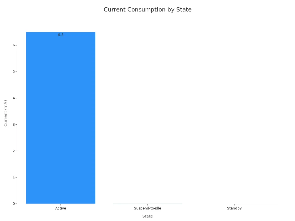
Two board-level traps ruin your readings:
The J-Link debugger can keep the chip awake because the debug interface prevents deep sleep. Disconnect the debugger or power the board from a battery while measuring.
The UART peripheral, if not suspended, keeps clocking and prevents µA-level current readings. This is the top reason people think Zephyr PM “doesn’t work.”
A microampere standby current only appears when every peripheral, debug path, and leaky component is truly off.
Board leakage also matters. Resistor dividers, pull-ups on unused pins, and reverse leakage in diodes all add up. Audit every path to ground before you trust a low-power architecture on paper.
Battery and regulator choice set the floor. Pick a regulator with low quiescent current, and match the cell chemistry to your temperature range. Dynamic power control in firmware helps, yet the hardware budget decides the outcome. This low-power wireless technology only delivers long battery life when the board itself stays quiet. Apply chip-level energy efficiency optimization at the rail, and your energy efficiency gains will hold in the field.
Interface Design and Sensor Integration
Your BLE radio can only work as well as the buses that feed it. A noisy sensor line or a long I2C run can damage data before the radio ever sends it. Design each interface for its real distance and load.
SPI, I2C, and UART Interfaces
Match the bus to the job. SPI stays on one PCB, usually within about 10 cm. The host controls the clock, so you get low overhead and high throughput for local links. SPI has no built-in arbitration and no addressing. Give each slave its own chip-select line.
I2C is a two-wire bus with software addressing and true multi-controller arbitration. Standard mode runs at 100 kbit/s, Fast at 400 kbit/s, Fast-mode Plus at 1 Mbit/s, and High-speed at 3.4 Mbit/s. Keep the bus load inside the roughly 400 pF capacitance limit per NXP specs. Repeaters, buffers, and extenders can stretch I2C into the tens of meters, but treat that as a planned extension, not a default.
bhazi | Typical max bus length | Arbitration / topology |
|---|---|---|
SPI | Usually confined to a single PCB (~10 cm) | 1 master / many slaves with dedicated CS per slave; no built-in arbitration |
I2C | ~1 m (standard) | Multi-drop bus, 1 master / many slaves; supports multi-controller arbitration |
UART | Short and implementation-dependent (TTL) | Point-to-point; no arbitration |
UART is point-to-point with no arbitration. Raw 3.3 V TTL works for short local runs. Add RS-232, RS-422, or RS-485 transceivers when you need more distance. TI RS-485 data shows tests at 50 m, 100 m, 150 m, 200 m, and up to 1000 m depending on data rate and transceiver. Add level shifting wherever your sensor and your BLE SoC use different rails. Size pull-ups based on bus capacitance, not habit.
EMI/EMC and Sensor Integration
DC-DC converters are the main source of electromagnetic noise in midziyo yeindasitiri. Cables and metal enclosures act like unintended antennas and send that noise outward. Stop emissions at the converter, then block them from spreading through cables and enclosures.
Inserting a choke-coil noise filter into the DC output line of a DC-DC converter improved minimum LTE receiver sensitivity during robot operation by approximately 11 dB.
The filter sent high-frequency converter noise back into the converter through its impedance. A small 1.6 × 0.8 × 0.8 mm, 1.3 A-rated inductor did the job. Ferrite beads are other options, picked by how much noise suppression and current superposition behavior you need.
Clean up the sensor signal before it reaches the BLE protocol stack. An analog front end matches conditioning to each sensor’s output. Integrated signal processing puts amplification, filtering, conversion, temperature compensation, and digital processing into one IC. That shortens the noise-prone discrete path. The flow runs: amplify, filter, convert, calibrate, then transmit over SPI, I2C, or bluetooth yakaderera simba.
On the software side, keep one API layer over each bus. Return clear error codes for timeouts and bus faults. Check payload lengths before you hand data to the BLE stack. Apply application-layer security to sensor data, since BLE link encryption alone does not cover your cloud path.
Stackup, Materials, and DFM Trade-offs
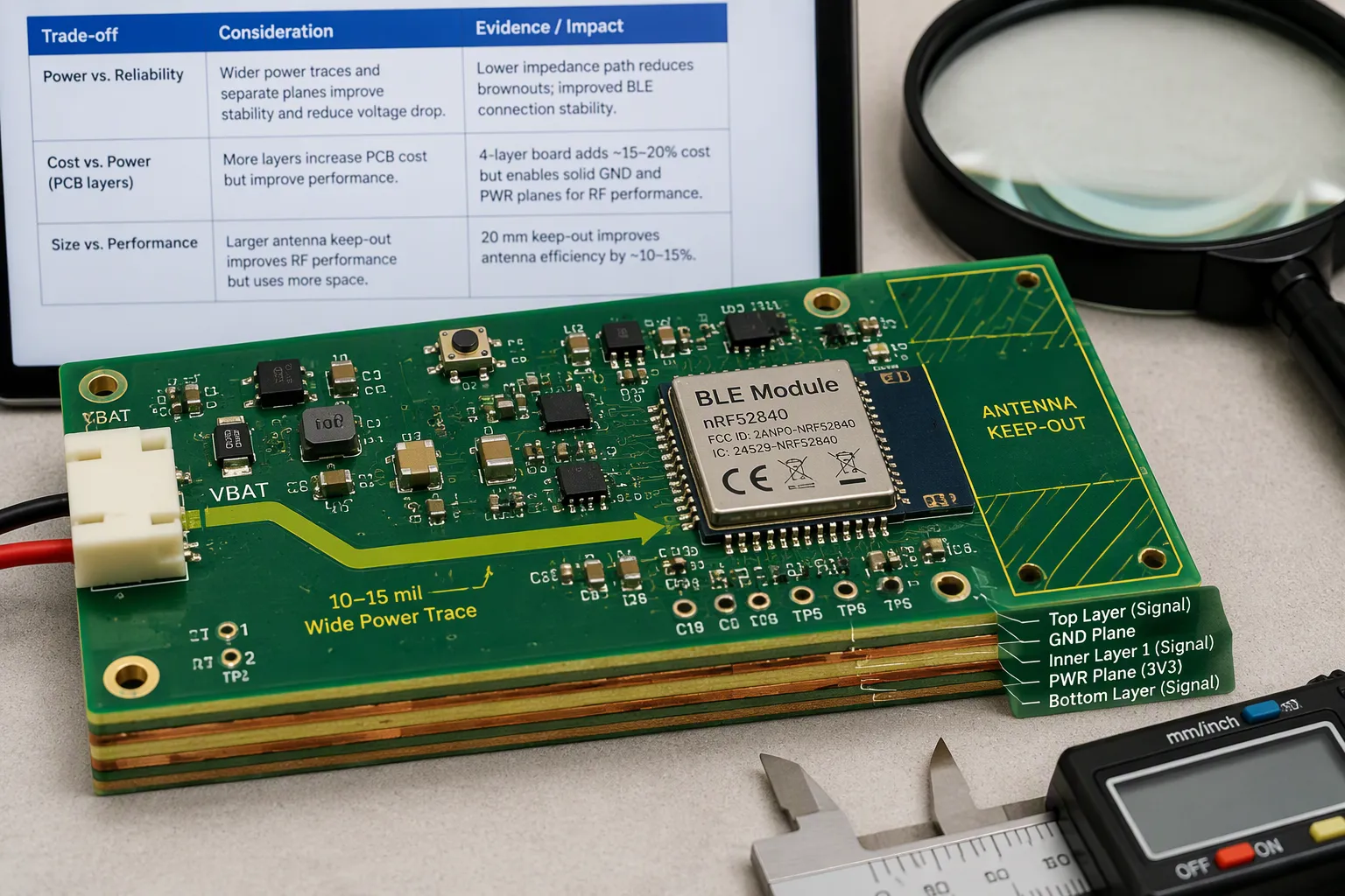
Stackup and Material Selection
Your stackup decides how well the BLE radio works and what the board costs. A four-layer board with its own power and ground planes can cut power loss by up to 15% compared to a single-layer design with shared ground traces. That gain helps you use less power without changing any firmware. Single-layer boards cost less, but they can’t give a BLE design a clean RF reference plane.
Pick the dielectric for its loss and its price. Standard FR-4 works for most 2.4 GHz BLE boards. Lower-loss materials only help when your traces are long or your margin is thin. Keep the RF layer next to a solid ground plane, and keep that plane unbroken under the antenna feed.
DFM Constraints and Design Checklist
Follow your fabricator’s minimum trace width and spacing. Keep power traces short and wide, at 10–15 mils for up to 1 A. Boards smaller than 30 mm x 30 mm make wide traces and big power planes hard, so plan the layout early. Place vias inside pads only when your assembly house supports via-in-pad fill. Respect component clearance around the antenna keep-out, and check how panelization rails and breakaway tabs sit near the RF edge. A rail that crosses the keep-out can shift your tuning and lower RF yield.
Every BLE design trades one goal against another. Use this table to set priorities before layout.
Tengesa | Uchapupu |
|---|---|
Power vs. Reliability | Lowering BLE output power from +4 dBm to 0 dBm can cut current draw by nearly 30%, but minimizing transmission power may cause connection issues in noisy environments. |
Power vs. Performance | Reducing sensor sampling rates saves power but can compromise data accuracy; batching readings (e.g., every 30 s instead of every second) cuts MCU active time by up to 95%. |
Cost vs. Power (PCB layers) | Single-layer PCBs are cheaper but insufficient for complex designs; 4-layer boards with dedicated power/ground planes can reduce power loss by up to 15% versus single-layer designs with shared ground traces. |
Power vs. Cost (component selection) | A well-chosen PMIC achieves voltage-conversion efficiencies above 90% versus 70–80% for less optimized solutions; dynamic voltage scaling can cut MCU power draw by 20–30%. |
Power vs. Range/Space | Compact boards (<30 mm x 30 mm) make wide traces and extensive power planes difficult; long/narrow traces raise resistance and heat loss, so power traces should be kept short and wide (10–15 mils for up to 1 A). |
Some links accept lower data rates to win range and battery life. That logic applies to BLE too.
LoRa achieves its combination of range, robustness and low power consumption partly by accepting relatively low data rates… sacrificing bandwidth that isn’t needed in exchange for greater range and lower power consumption can be an excellent engineering trade-off.
Before you release the design, confirm five things. Your stackup gives the BLE radio a solid reference plane. Your antenna keep-out survives panelization. Your power traces meet the current budget. Your regulator quiescent current fits the sleep budget. Your energy efficiency targets match measured current, not datasheet hopes. These checks protect power efficiency and battery life at volume.
Low-power BLE communication comes from two habits: steady duty cycles and careful control of sleep current. Industrial reliability comes from board-level choices—SoC or module, RF layout, power integrity, and DFM-aware design. Start by measuring sleep current on a real board early. Plan the RF keep-out before placement, following the module datasheet for the exact zone and extending it past the board edge. Check your stackup against EMC needs, not cost alone. Then test under real industrial conditions and manufacturing tolerances. Lab benchmarks will not show you how ble power efficiency and long battery life hold up in the field.
FAQ
How do I choose an advertising interval for a battery-powered sensor?
Start with your latency need, then stretch the interval as far as the application allows. A 1 s interval draws roughly 9.4 µA on average, and a 10 s interval drops that to about 2.3 µA. Longer intervals save ble energy, but they slow down discovery and reconnection.
Should I use a pre-certified module or a discrete BLE SoC?
Pick the module when schedule and certification risk matter more than unit cost. A module arrives with the radio, crystal, and antenna already tuned, so you skip RF certification work. Choose a discrete SoC only when high volume justifies the layout effort and your team owns RF test equipment.
Why does my board still draw milliamps in sleep mode?
Check three things first. The debugger can hold the chip awake, so disconnect it. An unsuspended UART keeps clocking and blocks microamp readings. Leaky pull-ups and resistor dividers also add current. Audit every path to ground before you blame the ble protocol stack or the firmware.
How much RF keep-out does the antenna really need?
Follow the module datasheet for the exact zone, and extend it past the board edge. Keep the ground plane unbroken under any 50-ohm trace. Stitch the RF ground with vias at 2–3 mm spacing near the keep-out. A broken keep-out costs link budget that no firmware setting can recover.