You get high-efficiency power conversion and steady regulation from one habit: match every design choice to the real load, the real thermal path, and the real board you can build. Two goals drive your work. You want the highest power conversion efficiency you can reach. You also need output voltage to stay flat when the load moves. These goals pull against each other. More efficiency often means more switching, and more switching can disturb the output. Your job is to balance them with data, not guesswork. Good power conversion systems come from careful choices at every stage. Every gain in efficiency and every point of regulation depends on that balance.
主要なポイント(要点)
Choose the right converter type for your needs: buck lowers voltage, boost raises it, and buck-boost handles inputs that change.
Use a switching regulator instead of a linear one when the power loss is more than 2 watts. This saves energy and lowers heat.
Design your control loop to have at least 60 degrees of phase margin. This helps keep the output voltage steady when the load changes.
Pick parts like inductors and MOSFETs by weighing trade-offs, such as resistance and gate charge, for your switching frequency.
Test your design carefully with honest measurements. This makes sure efficiency and regulation targets hold in production.
電力変換トポロジの選択
Buck, Boost, and Buck-Boost Trade-offs
あなたは始める choosing a topology with three inputs: load profile, input-to-output voltage ratio, and isolation needs. A regulator works best when VIN equals VOUT, and it loses efficiency as that ratio grows. With an input moving between 36 and 60V, a 48V bus is best, because it carries 4× less current than 12V and cuts PDN losses by about 16×. That input can drop below 48V, so this stage must be a buck-boost.
トポロジー | 電圧比 | 分離 | ベストフィット |
|---|---|---|---|
降圧型 | 階段を下りる | いいえ | Simple, low-cost rails; discontinuous input current raises EMI |
ブースト | Steps up | いいえ | Continuous CCM current; suits active power factor correction |
昇降圧型 | 上または下のステップ | いいえ | Battery-powered systems with drifting input |
Buck converters are the simplest and cheapest choice, and they reach high efficiency at high power. Boost stages draw continuous current in CCM, which makes them great for active power factor correction. Buck-boost stages handle a changing input, but they flip the output and their switch has no ground reference. Where efficiency and flexibility matter, dc-dc converters replace linear regulators. Isolated regulated converters reach high efficiency in small footprints.
Synchronous Rectification Basics
You should swap the freewheeling diode for a MOSFET to cut conduction losses on low-voltage, high-current rails. The diode drops a fixed forward voltage at any current. A MOSFET drops current times RDS(on), so the loss goes down as you parallel devices or pick a lower-resistance part. This one change often decides whether a power converter meets its efficiency target.
Isolated Topologies and When You Need Them
Pick an isolated topology when safety or ground separation requires it. The flyback is the simplest isolated option at low power, yet it performs poorly above about 10A. A forward converter adds an output inductor and handles high output currents better. Advanced power converter topologies, including two-switch buck-boost stages, boost efficiency at the cost of more complexity.
Note: Poor regulation usually means higher losses, so treat a drifting output voltage as an efficiency warning.
Power Conversion Efficiency and Loss Mechanisms
Switching vs. Linear Losses
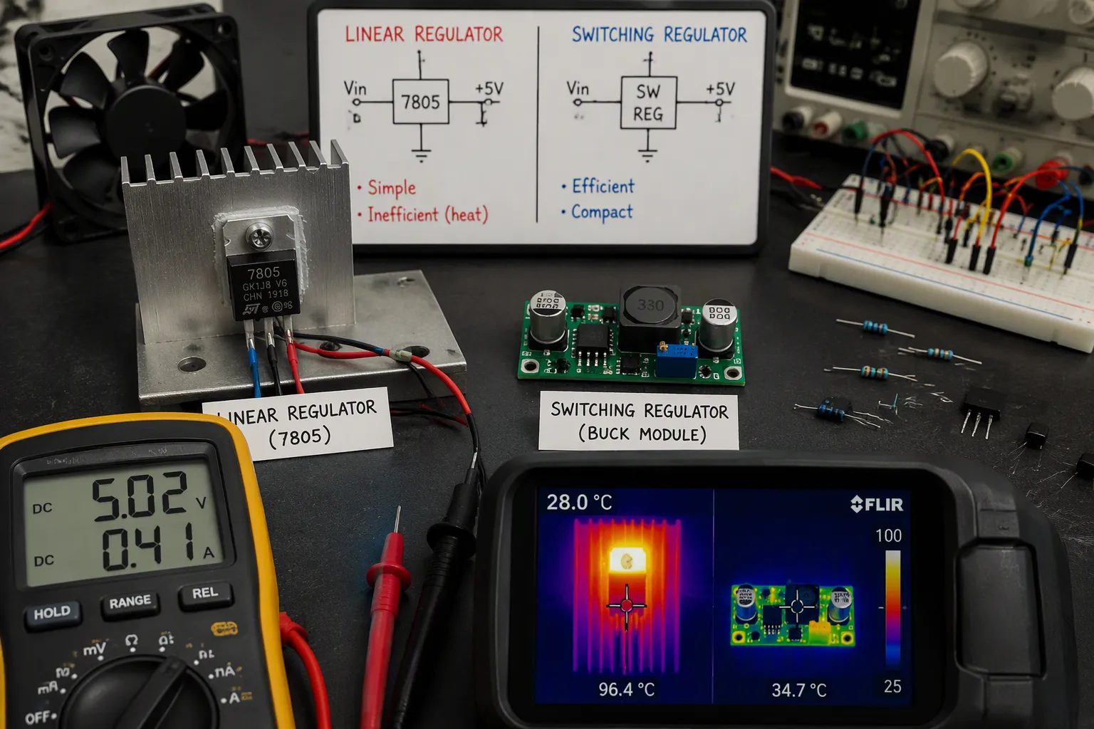
A linear regulator keeps its output steady by dropping the extra voltage between input and output. The load current flows through both the load and the regulator. So the wasted power equals the voltage drop times the output current. In a common car 5V regulator fed from a 14.3V charging system, the drop is 9.3V. At 1.0A the load gets 5W while the regulator burns 9.3W, which gives an efficiency of only about 35%. Switching elements avoid this waste. They chop the input and store energy in an inductor, so they lose only a small part of the delivered power. That is why switch-mode power supplies reach high efficiency where linear parts cannot.
| リニアレギュレータ | スイッチングレギュレータ |
|---|---|---|
効率化 | Low (30–60% when VIN is far above VOUT) | 高(80~95%) |
熱応力 | High for large VIN–VOUT or high current | Low for the same load |
標準負荷電流 | 最大500mA | 1 A to 10 A and beyond |
You should treat the 2W rule as a practical threshold. Calculate loss as (VIN − VOUT) × IOUT. If the result is over 2W, pick a スイッチングレギュレータ. If it stays at or below 2W, a linear part may work with proper heatsinking. Supplying 5V at 2A from 12V with a linear regulator wastes 14W, which is not practical. A 90% efficient switching stage wastes close to 1W for the same job.
A 7805 running from 12V at 500mA makes over 3.5W of heat. That part needs a heatsink or better PCB thermal design.
Loss Breakdown Across the Load Range
Four loss terms shape power conversion efficiency, and each one scales in a different way. Conduction loss rises with the square of load current, so it rules at heavy load. Switching loss stays roughly proportional to frequency and bus voltage, and it rules at light load. Gate-drive loss scales with frequency and gate charge. Quiescent loss stays fixed, so it matters most when output current is tiny. Advanced designs have shown over 99.1% peak efficiency by combining component, topology, and control innovations.
Light-Load Efficiency Modes
Under fixed-frequency PWM the switching count stays constant, so self-consumption stays constant and efficiency falls at low current. Light-load modes fix this. Burst, skip, and PFM control stretch the period and cut the number of switching events per unit time. At a 1mA load, forced PWM gives only about 8% efficiency, while PFM reaches roughly 84%. PFM also removes high-side turn-on loss and cuts gate-drive and dead-time loss. Zero-crossing detection adds another gain by turning off the low-side FET when inductor current goes negative.
Tip: PFM brings variable frequency, higher ripple, and possible audible noise. Check EMI behavior before you commit.
Voltage Regulation and Control Loop Design
Feedback Compensation and Stability
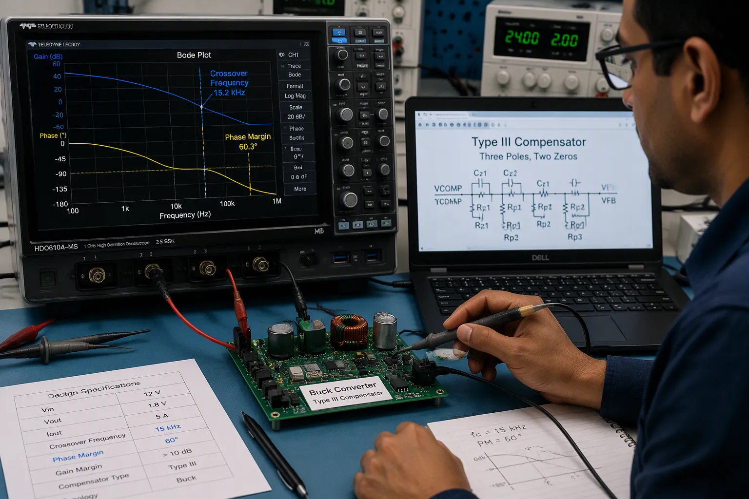
考える 制御ループ as the part of the dc/dc converter design that decides whether the output stays steady or wobbles. A buck, boost, or buck-boost stage all need the same three jobs from the compensator. First, high gain at DC works like an integrator. It boosts any steady error until the duty cycle fixes it. Without that integrator, proportional-only control leaves a steady-state error. Second, two zeros near the LC resonance lift the phase at crossover. Third, two high-frequency poles cut the gain above crossover. They keep switching ripple and injected noise from changing the duty cycle.
A Type III compensator (three poles, two zeros) provides all three. The table below shows a worked buck example.
対価 | Value / Placement | 目的 |
|---|---|---|
クロスオーバー周波数 | 15 kHz (about fsw/10) | Fast transient response within averaged-model validity |
Phase margin target | ≥ 55° (design achieves 60°) | Clean transient, headroom for part variation |
Gain margin target | ≥12dB | Margin against parasitic phase lags |
Compensator zeros | 3.2kHzおよび6.2kHz | Recover about 38° of phase at crossover |
Compensator poles | 75kHzおよび145kHz | Roll off gain; attenuate ripple and noise |
Loop gain slope at 0 dB | −20 dB/decade | Single-crossover stability |
Phase margin sets overshoot directly. At about 65° you see roughly 5% overshoot and settling in a couple of cycles. At 45° overshoot climbs to about 20% with moderate ringing. At 25° it reaches about 50% with long ringing. You should aim for 60° and never go below 45°, because the extra margin absorbs drift from temperature, age, and manufacturing variation.
A loop that measures 60° of phase margin on the bench can still oscillate once you add an input filter. The filter and converter interact through impedance, not through the loop you just compensated. That failure shows up at the filter’s resonance (see Middlebrook Stability Criterion).
Transient Response and Remote Sensing
Fast load steps, such as 10 mA to 500 mA in nanoseconds, need high loop bandwidth, a fast error amplifier, and strong phase margin across load and output capacitance. You should pick low-ESR MLCCs for the output. Too aggressive compensation risks instability; too slow gives overshoot and undershoot. Raising output capacitance improves transient behavior but costs board area and startup time. One technique pushes the unity-gain frequency higher with a small constant-current OTA driving a high-impedance node, which widens bandwidth while load conditions barely affect stability.
For a line and load regulated output across long traces, add remote sensing. A dedicated sense pair wires directly to the load terminals in a Kelvin connection, separating voltage detection from the high-current path. Those lines carry only a tiny bias current, so their own IR drop is negligible. The feedback loop then compares the sensed voltage with its internal reference and raises the output until the load sees the set-point. This corrects trace, cable, and connector resistance, giving precise regulation and a stable power supply even under dynamic demand.
ヒント: Route sense lines as a tight differential pair away from switch nodes. A noisy sense line corrupts output-voltage regulation more than any compensator tweak can fix.
Component Selection for Overall Efficiency
Inductors, Capacitors, and MOSFETs
あなたがすべき pick the inductor size by checking three limits at the same time. Choose the nominal inductance from the ripple factor at worst-case input and light load, then round up to the nearest standard value. Check the saturation current at 30% roll-off against peak current, and keep 20–30% margin. Make sure the rated current covers the RMS value, and read the DC-bias and temperature-rise curves before you decide.
Output capacitor choice usually follows the load step, not the ripple. A 3% transient dip can need far more capacitance than a 1% ripple budget. Check ESR, RMS ripple current, and package size together.
MOSFET selection is a balance, not a race to the lowest RDS(on). Gate charge grows with die size, so a low-resistance part often has high Qg and slows switching. Weigh RDS(on) against Qg and Miller charge at your target frequency.
デバイスの選択 | 第3章:濃度 | トレード・オフ |
|---|---|---|
Low RDS(on) MOSFET | 低伝導損失 | High Qg, slower edges |
Low Qg MOSFET | 高速スイッチング | 伝導損失の増加 |
Controllers and Gate Drivers
Higher gate drive voltage, such as +15V/-5V, makes sure the gate turns on solidly and protects the gate oxide. It also needs tighter regulation from the driver supply. Active gate control shapes dI/dt and dV/dt to cut switching loss while keeping EMI in check, but it costs sensing bandwidth and adds complexity.
Watch the gate loop. Parasitic inductance causes ringing and false triggering, which raises losses. Keep traces short, use a Kelvin source, and place decoupling close to the driver.
Tip: Gate charge loss is small against the power rating, but it heats the driver and external Rg. Give those parts thermal headroom.
Package-Embedded Inductors for Integrated Regulators
Package-embedded magnetic core inductors are a new option for buck integrated voltage regulators. Tightly coupled shared-core islands raise inductance density to 250 nH/mm² and current density to 10 A/mm². In a 10-module converter at 40 A, coupled arrays gained 5.65% average efficiency over uncoupled baselines, with the best modules reaching 11.04%.
This matters for high-efficiency power conversion in high-step-down rails, such as 12 V to 1 V. Putting passives into the package lifts efficiency where board area is tight. Treat these parts as a design lever for power conversion systems that need compact, high efficiency delivery.
Efficiency, Size, and EMI Trade-offs
Switching Frequency and Thermal Management
You pick switching frequency first, because it affects every other choice. A higher frequency makes inductors, capacitors, and filters smaller, and it raises power density. That same change adds more switching events each second, so losses go up and efficiency may fall when thermal design is weak. Sharper dv/dt and di/dt also raise conducted and radiated noise. You then need tighter layout, better filtering, and careful gate-drive tuning.
デザインの優先順位 | Effect of Higher Switching Frequency |
|---|---|
効率化 | More switching events each second; total efficiency may drop without strong thermal design |
Solution Size | Smaller passives and higher power density; passives become more sensitive and costlier |
Sharper edges raise noise; needs tighter layout, shielding, and filtering | |
サーマル | More junction temperature cycling and derating needs |
Estimate switching losses at your candidate frequency, then check thermal headroom in the module and heatsink. Validate dv/dt and di/dt control for EMI risk, adjust, and repeat. Confirm with simulation, thermal test, an EMI scan, and a load test before you finalize.
Tip: A frequency that passes EMI on the bench can still fail in a metal enclosure. Scan early.
Copper Area and DFM Constraints
Plan the heat path before you route. Thermal via arrays carry heat from surface parts into internal or backside copper planes, and filled or plugged vias prevent solder wicking. Heavy copper cuts resistive heating and spreads heat sideways. Copper coins and insulated metal substrates serve devices where via arrays fall short. Group vias into farms, and follow IPC-7093 for bottom-terminated packages and IPC-2152 for current-carrying width.
DFM then limits the plan. Large copper areas pull heat from solder joints during reflow, so size pours around the real heat path. Minimize solder paste to stop component floating. Keep high-current traces away from sensors and op-amps.
Cost and BOM Trade-offs
Lower frequency keeps GOOD and EMI control cheaper. Higher frequency may raise cost through advanced devices and tighter EMI control. Weigh each option against your load profile, not against a datasheet peak.
Note: Every gain in high efficiency costs board area, cost, or EMI margin somewhere.
Board-Level Implementation and Testing
Hot Loop and Switch Node Layout
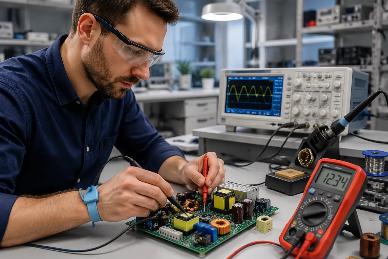
The hot loop is the high-current path that carries switching current. Its area sets parasitic inductance, and parasitic inductance sets ringing, overshoot, and EMI. You should place input and decoupling capacitors just millimeters from the MOSFET half-bridge. A smaller loop area lowers loop inductance and cuts voltage overshoot. A vertically oriented power loop in a multilayer board shrinks loop area even more, and layouts like this have reported overshoot reduction of up to about 4 V compared with ordinary layouts.
デザインアクション | に適用されます | 効果 |
|---|---|---|
Capacitors close to MOSFETs | Hot loop | Shrinks loop area, lowers inductance |
Vertical power loop in multilayer PCB | Hot loop | Cuts loop area and overshoot |
Laminated busbars for DC-link | Hot loop | Prevents V_DS overshoot at turn-off |
Compact, isolated gate loops | Switch node | Stops false turn-on from Miller coupling |
Matched source inductance in parallel devices | Switch node | Avoids uneven current sharing |
You should also keep reference planes unbroken and keep noisy switching areas away from sensitive analog areas. These steps hold back high dv/dt and di/dt noise and protect signal return integrity.
Measurement and Validation
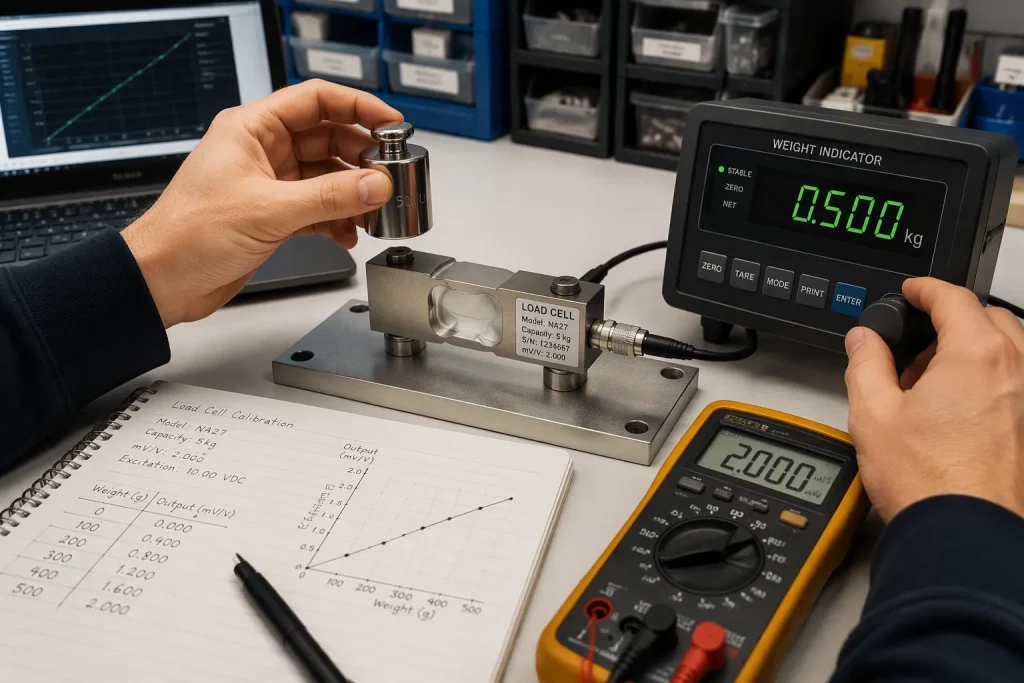
Bench data only helps when the setup is honest. Calibration error grows with the reading, so large values carry larger absolute errors. Zero offset adds a constant error that hurts small readings most. Instrument drift, lag time, and hysteresis all shift results. You should re-zero the meter at the start, wait for stability before each reading, and sweep in one direction only.
間違い | How It Skews Readings | 避ける方法 |
|---|---|---|
キャリブレーションエラー | Grows with full-scale value | Verify against a precise reference |
ゼロオフセット | Constant error, worst at small values | Re-zero and record the offset |
Lag time / hysteresis | Early readings sit too high or low | Wait for stability; sweep one way |
環境騒音 | Drafts and vibration bias results | Shield or control the workspace |
Validate transient load steps, line and load regulation, and efficiency before volume manufacturing. Remember that regulation and losses move together. A transformer with 7% impedance showed 11 kW of load losses and 98.6% efficiency, against 8 kW and 98.9% at 5% impedance. Poorer regulation means higher losses, so treat a drifting output voltage as a warning about power conversion efficiency.
Tip: Take multiple readings across the widest range. Variation you never measured is variation you cannot fix.
High-efficiency power conversion and steady regulation come from one connected chain: topology, control loop, components, layout, thermal design, and DFM all matched to your real limits. You can’t avoid trade-offs. The best design fits your own load profile, thermal envelope, and cost target, not a datasheet peak.
Note: Bench data beats guesses every time. Measure, iterate, then validate before volume manufacturing.
Treat every gain in power conversion efficiency as a measured result, not a hope. Careful power conversion work earns you a reliable power supply. Build reliable power supplies the same way, one honest measurement at a time, and your efficiency and regulation targets will hold in production.
FAQ
How do you choose between buck, boost, and buck-boost?
Start with three inputs: load profile, input-to-output voltage ratio, and isolation needs. Pick a buck to step down, a boost to step up, and a buck-boost when the input drifts above and below the output. Add an isolated topology only when safety or ground separation demands it.
Should you use a linear regulator or a switching converter?
Calculate the loss as (VIN − VOUT) × IOUT. If the result stays at or below 2W, a linear part may work with proper heatsinking. Above 2W, switch to a switching stage. A linear regulator fed from a much higher input burns most of the delivered power as heat.
How do you keep the control loop stable?
Aim for at least 60° of phase margin and never drop below 45°. Set crossover near one-tenth of the switching frequency, and use a Type III compensator to lift phase at the LC resonance. Then re-check stability with your input filter connected.
Tip: A loop that looks clean on the bench can still ring once the input filter interacts with it.
Why does efficiency collapse at light load?
Fixed-frequency PWM keeps switching at the same rate no matter how small the load is, so self-consumption stays constant. Burst, skip, and PFM modes cut the number of switching events and recover much of that loss. Check EMI and ripple before you enable them.
Keep measuring, keep iterating, and your efficiency and regulation targets will hold up in production.