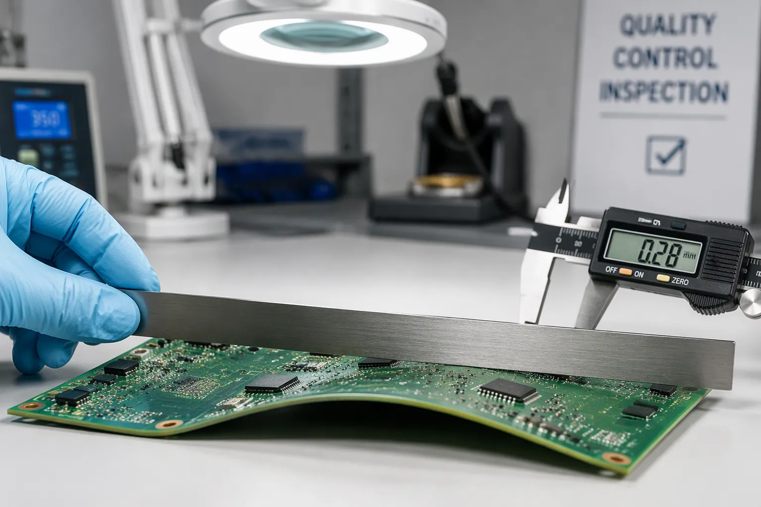
Bow and twist describe flatness failures. Bow is a curvature where the four corners stay in one plane while the center bends inward or outward. Twist is a diagonal deformation where one corner lifts out of the plane of the other three. IPC-6012 and IPC-A-600 set the reference: 0.75% maximum for SMT boards, 1.5% for through-hole-only boards, and 0.50% for strict designs.
Flatness affects every stage of a PCB’s life. A warped board fights enclosure fit, misaligns fasteners, and stresses solder joints. Stakes become clear when you separate challenges from causes. Intrinsic causes live in the board’s design and fabrication. Extrinsic causes arrive through storage, handling, and assembly. Solutions follow the same split.
Основные выводы
Bow bends the board’s center. Twist lifts one corner. Both make the board uneven.
IPC sets flatness limits: 0.75% for SMT boards, 1.5% for through-hole boards, and 0.50% for strict designs.
Warped boards cause assembly defects like tombstoning and bridging. They also hurt product fit and reliability.
Intrinsic causes come from design and fabrication. Extrinsic causes come from storage, handling, and assembly.
Measure bow and twist using IPC-TM-650 Method 2.4.22. Rest the board on three points over a flat surface.
Design solutions include mirror-symmetrical stackups, balanced copper, and matching CTE values.
Process solutions include controlled lamination, baking, and tuned reflow profiles.
Track flatness as a metric. Log measurements and watch for trends to prevent defects.
What Are PCB Bow and Twist?
Bow Versus Twist
Bow as Center Curvature
Bow is a curvature in which the four corners of the board stay in one plane while the center bends inward or outward. Picture a board resting on a flat table with all four corners touching the surface. If the middle arches up like a shallow dome, or sags down like a bowl, you have bow. The deformation runs along one axis, so the board looks like a section of a cylinder rather than a flat plate.
Twist as Diagonal Lift
Twist is a diagonal deformation in which one corner lifts out of the plane of the other three. Set the board on a flat surface and press down three corners. A twisted board rocks, and the fourth corner rises off the table. The warp runs corner to corner across the diagonal, which makes twist easy to spot during handling but harder to correct than simple bow.
IPC Acceptability Limits
SMT Versus Through-Hole Limits
IPC-6012 and IPC-A-600 give you the shared reference for acceptable flatness. The maximum allowable bow and twist is typically 0.75% for surface-mount boards and 1.5% for through-hole-only boards. The percentage expresses the maximum deviation divided by the board length, so a longer board tolerates a larger absolute gap at the same percentage.
Strict-Design Caps
Some designs cap the limit at 0.50%. Fine-pitch and BGA assemblies, thin boards, and products with tight mechanical tolerances often fall into this group. Confirm the applicable class and limit with your fabricator and assembler before you release the design, and record the agreed value on the fabrication drawing.
Почему плоскостность имеет значение
Assembly and Manufacturing Impact
A warped board disrupts the assembly line. Paste deposition varies across an uneven surface, placement machines lose their reference height, and reflow ovens struggle to heat a board that does not sit flat. Automated feeders, test fixtures, and connector seating all depend on a predictable board plane.
End-Use Fit and Reliability
Flatness also decides whether the finished product fits together. A bowed board misaligns fasteners, strains enclosure walls, and leaves gaps at mounting points. Residual stress from warpage can release during thermal cycling in the field, and that movement works against solder joints over the product’s life.
Проблемы и последствия
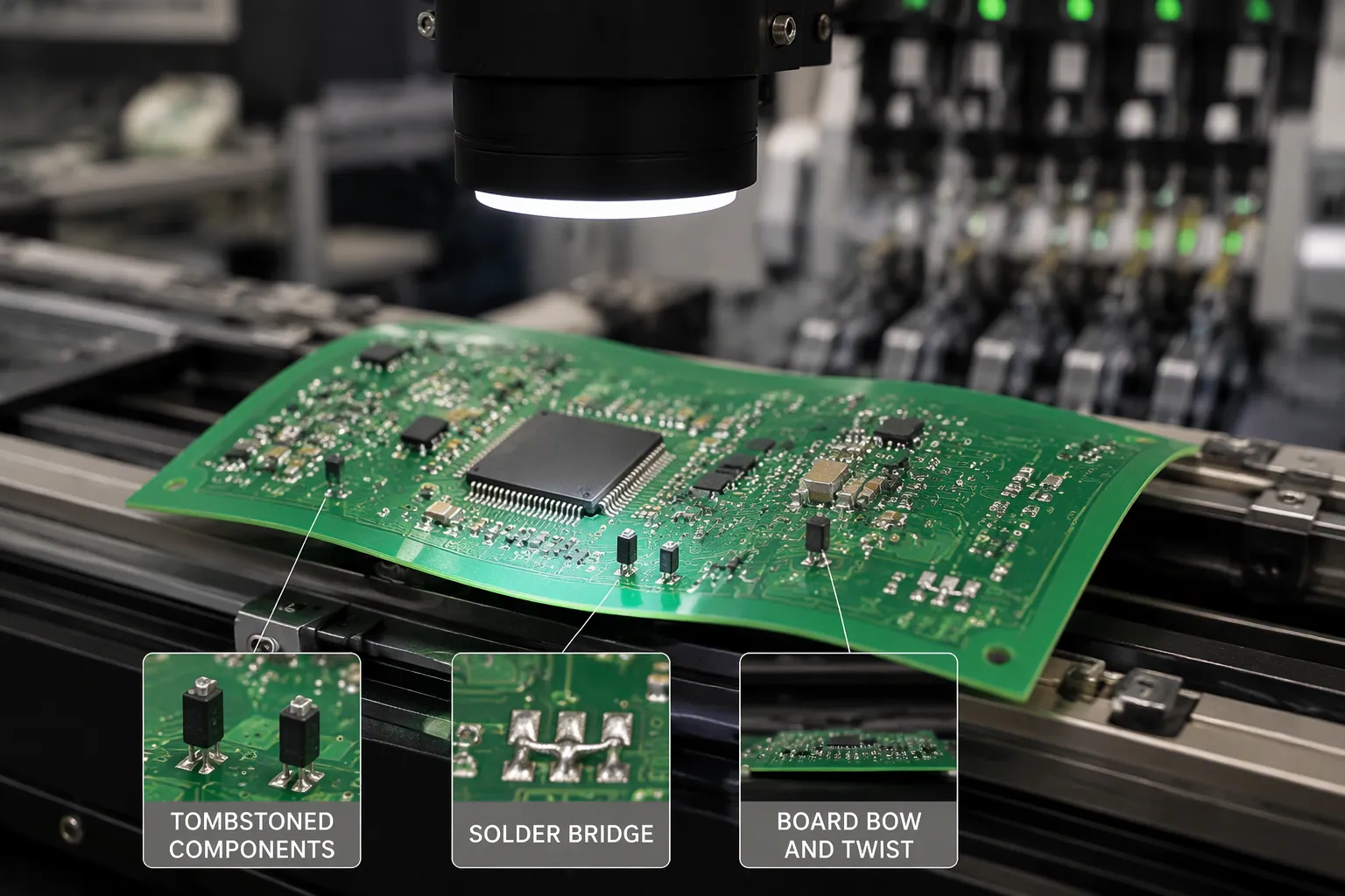
Warpage rarely stays a cosmetic problem. It travels through the сборочная линия and into the field, and each stage exposes a different failure mode. You can group these impacts into three areas: soldering, inspection and handling, and geometry-driven risk.
SMT Assembly Defects
Placement Misalignment and Bridging
A warped board changes the distance between the stencil and the pad. Paste deposits grow uneven across the panel, and the placement head loses its height reference. Fine-pitch packages and BGAs suffer first. A slight tilt pushes a lead onto a neighboring pad, and solder bridging follows. Open joints appear where the gap grew too wide for the paste volume to span. Both defects escape easily on a board that looked acceptable at incoming inspection.
Tombstoning and Lifted Components
Small two-terminal parts behave like seesaws on an uneven surface. One end of the molten solder pulls harder than the other, and the component stands up — the classic tombstone. Larger parts lift at one edge instead. The joint forms on one side and stays open on the other. Reflow cannot compensate for a board that does not sit flat, and rework on these joints costs time and risks pad damage.
Residual stress adds a slower failure. Internal stress locked in during fabrication can release during reflow or during field thermal cycling. The joint absorbs that movement, and fatigue cracks develop over the product’s life. A board that passed functional test can still fail in the field months later.
Inspection and Handling Issues
AOI False Errors and Feeder Jams
Automated optical inspection assumes a known focal plane. A bowed board shifts that plane across the panel, and the camera reports false errors on joints that are perfectly good. Operators then spend time reviewing phantom defects, and real defects hide in the noise. Handling equipment struggles too. Warped panels jam automated feeders, stick in test fixtures, and misalign in magazine slots. Each jam costs line time and risks mechanical damage to the board.
Connector Seating Problems
Connectors demand a flat mating surface. A twisted board tilts the connector housing, and the mating half seats at an angle. Contact force drops on one side, and the connection becomes intermittent under vibration. Press-fit connectors make this worse, because the pins must enter plated holes squarely. You may force the part into place and crack a barrel or lift a pad in the process.
High-Risk Geometries
Thin Boards and Large Panels
Some designs invite warpage by their physical nature. Thin boards lack the stiffness to resist bending, and large panels amplify any small curvature across a longer span. The percentage limit stays the same, but the absolute deviation grows with board length. A thin, large panel therefore needs tighter process control than a small, thick one.
High Layer Counts and Via-Dense Layouts
High layer counts stack more copper and more prepreg, and every asymmetric detail adds to the imbalance. Via-dense layouts concentrate metal in some regions and leave laminate exposed in others. Those regions expand and contract at different rates during heating and cooling. The result is a board that fights flatness from the moment it leaves the press.
Treat these geometries as early warnings. Flag them during design review, and give them extra attention at every process step.
Методы измерения
Метод 2.4.22 стандарта IPC-TM-650
Setup and Reference Plane
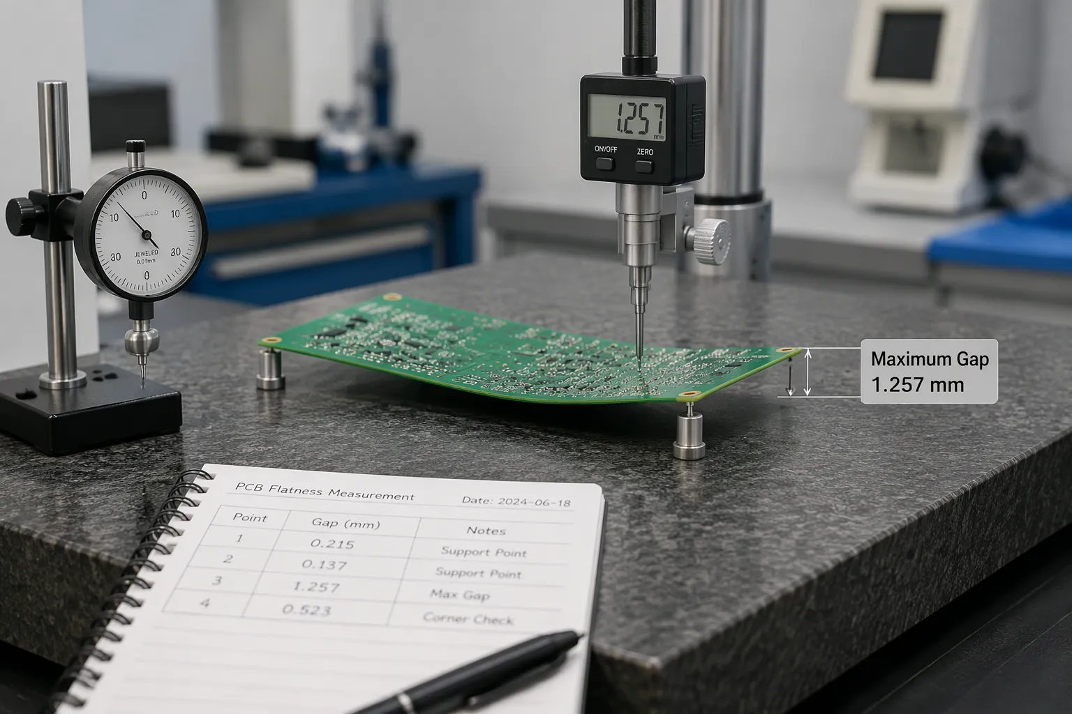
Метод 2.4.22 стандарта IPC-TM-650 gives you the industry procedure for quantifying warpage. You place the board on a flat reference surface, typically a granite table or a certified flat plate. The board rests on three fixed support points, and gravity alone holds it in place. No clamps, no weights, no pressure. The reference plane is the flat surface itself, and every measurement reads the gap between the board and that plane.
You then measure the maximum vertical deviation at the points where the board departs furthest from the reference. For bow, that point usually sits near the center of the panel. For twist, it sits at the lifted corner. A height gauge, dial indicator, or calibrated probe captures the reading. Record the location of each measurement alongside the value, because a single number without a position tells you little about the deformation pattern.
Calculating Percentages
The standard expresses warpage as a percentage rather than an absolute distance. You divide the maximum measured deviation by the relevant board dimension and multiply by 100. For bow, the divisor is the board length along the axis of curvature. For twist, the divisor is the diagonal length of the board. The result is the percentage you compare against the IPC-6012 and IPC-A-600 limits.
Work through one example. A board measures 200 mm long and bows 1.2 mm at the center. The calculation is 1.2 divided by 200, multiplied by 100, which gives 0.60%. That figure passes the 0.75% SMT limit but fails a 0.50% strict-design cap. Run the same math on the diagonal for twist, and report both values separately.
Measurement Pitfalls
Temperature and Support Effects
Measurement conditions change the result. A board measured straight off a warm press or out of a reflow oven reads differently than the same board at room temperature, because the laminate has not finished moving. Let the board stabilize at ambient conditions before you measure it. Support conditions matter just as much. A board resting on an uneven bench, or held by hand at one edge, distorts under its own weight and gives you a false reading.
Sampling and Documentation
One measurement on one board proves nothing about a production lot. Sample across the panel, across the lot, and at each stage — after fabrication, after reflow, and at incoming inspection. Document the method, the reference plane, the measurement points, and the ambient conditions alongside every result. That record lets you compare stages, spot trends before they become defects, and settle disputes with a fabricator or assembler using a shared, traceable basis.
Intrinsic Causes
Intrinsic causes originate inside the board itself. They take shape during design and fabrication, and they stay with the panel long after it leaves the press.
Stackup and Copper Imbalance
Asymmetric Layers and Odd Counts
A stackup with more copper or prepreg on one side of the centerline expands unevenly when heated. The thicker side moves further, and the board bows toward the thinner side. Odd layer counts make this worse, because no true center plane exists to anchor the balance. You can spot the risk on the fabrication drawing before any material is cut.
Split Planes and Uneven Copper Weight
Split planes and uneven copper weight concentrate metal in some regions and leave laminate exposed in others. Those regions expand at different rates during lamination and reflow. The board develops a permanent set that no reflow profile can remove. Review every power and ground layer for distribution balance, not just for electrical function.
Material and CTE Mismatch
Mixed Laminates and Prepreg Inconsistency
Every laminate carries its own coefficient of thermal expansion. Mixing materials with different CTE values forces the layers to move by different amounts as temperature changes. Inconsistent prepreg from lot to lot adds the same problem in smaller doses. The bond between layers absorbs that differential movement, and residual stress builds up in the panel.
FR-4 Versus PTFE and Rogers
FR-4 and high-frequency materials such as PTFE and Rogers laminates behave very differently under heat. A hybrid stackup that pairs them needs careful symmetry and a matched build. Each material fits its own application well, and the design must account for how they move together. Confirm the CTE values with your laminate supplier and document them in the stackup.
Lamination and Cure Issues
Press Pressure and Heating Cycles
неподходящий давление пресса leaves resin distribution uneven across the panel. Incomplete curing locks the laminate in a partially reacted state, and the board keeps moving after fabrication. Rushed heating and cooling cycles freeze stress into the panel instead of letting it relax. A controlled press cycle with a measured ramp and a full cure gives the laminate time to settle.
Blind and Buried Via Asymmetry
Blind and buried vias add metal in some layers and not others. A non-symmetrical via layout pulls the stackup in one direction during lamination. That imbalance survives every later process step. Place blind and buried vias symmetrically where the design allows, and flag any unavoidable asymmetry for extra flatness checks.
Extrinsic Causes
Extrinsic causes arrive after fabrication. Storage, handling, and сборка each add their own stress, and a board that left the press flat can still warp before it reaches the field.
Хранение и обработка
Moisture Absorption and Baking
Laminate absorbs moisture from the air. That moisture turns to steam during reflow, and the expanding vapor pushes the panel out of shape. A board stored in a humid room therefore carries hidden risk into the oven. Baking removes the moisture before assembly, and you should follow the laminate supplier’s bake schedule rather than guessing at a duration.
Packing and Depanelization Stress
Packing methods matter more than most teams expect. Boards stacked under heavy cartons or stored on edge can take a permanent set. Depanelization adds mechanical shock. Snapping a panel by hand bends the material around the breakaway, and the stress spreads into nearby circuitry. A routed or scored depanelization step with proper support keeps that stress local.
Assembly-Induced Warpage
Reflow Thermal Gradients
Reflow heats the board unevenly. The top surface sees the full oven profile first, and the bottom lags behind. That gradient makes one side expand before the other, and the panel bows during the cycle. Heavy asymmetric components pull the same way. A large connector on one edge adds mass and thermal lag, and the board curls toward it. Large cutouts and voids remove stiffness from one region, and the remaining material takes the load.
Fixturing and Connector Insertion
Fixtures and clamps hold a warped board flat by force. The board springs back once you release it, and the solder joints formed under clamp pressure now carry that stored energy. Connector insertion adds a direct mechanical load. Pressing a stiff connector into a thin PCB tilts the panel, and the pins enter at an angle. Support the board underneath during insertion, and check flatness again after the fixture comes off.
PCB Design Solutions
Design decisions set the flatness ceiling for everything downstream. You cannot fix an unbalanced stackup with a better reflow profile. Treat symmetry, copper distribution, and material choice as flatness controls from the first draft of the stackup.
Symmetry and Copper Balance
Mirror-Symmetrical Stackups
Build the stackup as a mirror around the centerline. Layer counts should be even, and each dielectric and prepreg thickness on one side should match its counterpart on the other. Place vias and cutouts symmetrically where routing allows. An asymmetric build expands unevenly during lamination, and the panel keeps that set permanently.
Copper Thieving and Hatched Fills
Distribute copper evenly across opposing layers, and target a balance within plus or minus 10% between them. Low-density areas need help. Add copper thieving, hatched fills, or matching breakaway copper so exposed laminate expands at the same rate as the dense regions. Review every power and ground plane for distribution, not just for current capacity.
Выбор материала и толщины
CTE Matching and Vendor Consistency
Match coefficients of thermal expansion where the design permits. Hybrid builds that pair FR-4 with PTFE or Rogers laminates need extra symmetry to absorb the differential movement. Stay with one laminate vendor across the product life. Prepreg varies from lot to lot, and a consistent source keeps that variation small.
Thickness and Rigidity Trade-offs
Thicker boards resist bending, and thin boards demand tighter process control. Weigh rigidity against weight, cost, and the mechanical needs of the enclosure. A thin, large panel amplifies any curvature across its span, so it deserves a stricter internal target than the 0.50% cap already noted for strict designs. Record the agreed limit on the fabrication drawing.
Технологические решения
Fabrication Controls
Lamination and Stress Relief
Оптимизировать lamination cycle before you chase defects downstream. Give the press a measured ramp and a full cure, and let the panel cool under controlled pressure. A rushed cycle freezes stress into the laminate, and that stress releases later during reflow. Build stress relief into the schedule as a deliberate step, not an afterthought.
Etch, Plate, and Bake Adjustments
Tune etch and plating so copper lands evenly across the panel. Uneven plating thickness pulls the board as it cools. Add a bake step after fabrication to relax residual stress and drive off absorbed moisture. Follow the laminate supplier’s bake schedule, and record the step on the traveler so every lot receives the same treatment.
Assembly and Storage Controls
Reflow Profile Tuning
Tune the ramp and soak stages to heat both board surfaces as evenly as the oven allows. A slow, balanced profile narrows the thermal gradient that bows the panel mid-cycle. Verify the profile with a profiler on the actual assembly, and recheck it whenever the panel design or component mix changes.
Moisture Management and Flat Storage
Bake boards when incoming inspection or storage history suggests moisture pickup. Store panels flat, in low-humidity conditions, and never on edge under heavy cartons. Choose a routed or scored depanelization method with proper support, and keep hand snapping away from dense circuitry.
Проверка и корректирующие действия
Flatness Checks and Trend Monitoring
Verify flatness per IPC-TM-650 Method 2.4.22 at fabrication and again after assembly. Log each reading with its measurement location and ambient conditions. Plot the results over time. A drifting trend warns you before a lot breaches the 0.75% SMT limit or a 0.50% strict-design cap.
Re-Bake and Re-Lamination
Mild warpage sometimes responds to a clamped thermal bake and cooling cycle. The clamp holds the PCB flat while the laminate relaxes, and the slow cool sets the new shape. Severe or persistent cases may call for re-lamination, depending on the board state and your design rules. Confirm the fix against the agreed limit before the lot ships.
Bow bends the center out of plane; twist lifts one corner off the diagonal. IPC-6012 and IPC-A-600 give designers and manufacturers one shared yardstick: 0.75% for SMT boards, 1.5% for through-hole-only boards, and 0.50% for strict designs.
Warpage rarely has a single source. Intrinsic factors such as stackup imbalance and cure stress stack on extrinsic ones such as moisture and reflow gradients. Attack them together at design, material, and process levels.
Build flatness checks into design reviews and incoming inspection. Measure per IPC-TM-650 Method 2.4.22, log every reading, and track bow and twist as a running process metric. Treat PCB flatness as a controlled variable, not an after-the-fact defect.
FAQ
What is the difference between bow and twist?
Bow keeps all four corners in one plane while the center bends up or down. Twist lifts one corner out of the plane of the other three, so the board rocks on a flat table. You measure bow along the board length and twist along the diagonal.
Which IPC limit applies to my board?
Match the limit to the assembly method. IPC-6012 and IPC-A-600 allow 0.75% for SMT boards and 1.5% for through-hole-only boards. Fine-pitch, BGA, and thin designs often need the 0.50% strict cap. Confirm the value with your производитель and record it on the fabrication drawing.
How do I measure bow and twist correctly?
Follow IPC-TM-650 Method 2.4.22. Rest the board on three fixed points over a flat reference surface with no clamps. Measure the maximum deviation, divide it by the board length for bow or the diagonal for twist, and multiply by 100. Let the board reach room temperature first.
Can I fix a warped board after reflow?
Sometimes. Mild warpage often responds to a clamped thermal bake and slow cooling cycle, which lets the laminate relax into a flat shape. Severe or persistent cases may need re-lamination. Verify the result against the agreed limit before the lot ships.
How do I prevent warpage at the design stage?
Build a mirror-symmetrical stackup with an even layer count. Balance copper across opposing layers, targeting within plus or minus 10%. Place vias and cutouts symmetrically. Match CTE values where possible, and stay with one laminate vendor to keep prepreg variation small.
Does copper balance really matter that much?
Yes. Uneven copper makes one region expand faster than another during lamination and reflow, and the panel keeps that set permanently. Review every power and ground plane for distribution, not just current capacity. Add thieving or hatched fills where laminate sits exposed.
Why does my board warp only after assembly?
Reflow heats the top surface before the bottom, and that gradient bows the panel mid-cycle. Moisture absorbed in storage turns to steam and pushes the laminate out of shape. Heavy asymmetric components and large cutouts add to the pull. Bake boards and tune a balanced reflow profile.
When should I reject a lot for warpage?
Reject when measured values exceed the limit agreed on the fabrication drawing. Log each reading with its location and ambient conditions, and plot results over time. A drifting trend warns you before a lot breaches the cap, so treat flatness as a tracked metric.