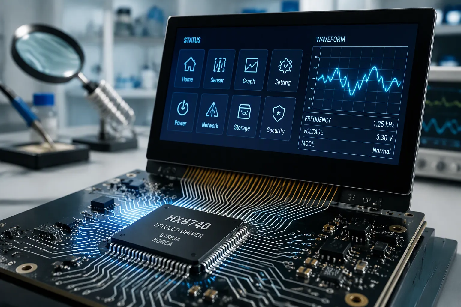
An LCD/LED display driver turns digital data into light. The driver ICs inside the module translate digital signals from the interface into analog voltages. Those voltages set each pixel’s brightness on the display. A separate path carries the data and timing pulses that keep every pixel in step.
Think of the division of labor this way: one side is the delivery route, and the driver is the translator at the door. One moves bits; the other converts them into the analog control each pixel needs. Driver ICs also run the control sequence for each frame. Neither half works alone.
You will see this partnership best by starting with the panel itself, then following color generation, signal timing, and a worked timing example.
Основные выводы
Driver ICs turn digital data into analog voltages that set pixel brightness.
Interfaces like parallel RGB, I2C, SPI, and MIPI DSI carry data and timing signals to the driver.
Timing parameters such as VSYNC, HSYNC, and porches must match the panel datasheet to avoid image problems.
LED drivers use constant current to keep brightness stable and PWM to dim without color shift.
Debug displays by checking one stage at a time and logging timing values for each board revision.
TFT Panel Structure and Operation
How a Thin-Film Transistor Controls a Pixel
You can think of each thin-film transistor as a tiny switch. Column and row wires connect to these switches, with one switch per pixel. The transistor passes current in one direction only. That one-way behavior keeps the charge on each pixel from draining away between refreshes.
Each pixel acts as a small capacitor. A layer of insulating liquid crystal sits between transparent conductive (ITO) layers, and this sandwich stores the charge. Here is the charge sequence for a pixel at row I, column J:
The TFT switch T(I,J) turns on.
The target voltage flows from the signal line D(I) to the pixel electrode.
The switch turns off once the electrode is fully charged, and the pixel capacitor holds the charge.
The data (column) driver supplies the target voltage, and the gate (line) driver controls the on/off switching.
During the ON stage (tON), a high gate voltage Vg charges the liquid crystal capacitor. The data voltage Vd becomes the pixel voltage Vp. During the OFF stage (tOFF), Vg is low and Vp holds steady. A small drop in Vp at the ON-to-OFF transition is called the feed-through voltage.
Panel Electronic Structure and Driver Placement
The panel carries two sets of wires. Gate lines run along the rows, and source (data) lines run along the columns. The gate driver circuit sits at the panel edge and pulses each row in turn. Source driver ics sit along the other edge and feed voltages into the columns.
These driver ics form the control system that links your host processor to the glass. The gate driver ics scan rows one at a time, and the source driver ics write data into the selected row. This arrangement lets the lcd/led display driver update every pixel in a fast, orderly sequence. Because the liquid crystal layer stores voltage, the display holds its image stably, and the control path can rewrite the voltage quickly through the TFT.
Driving Principle of an LED Screen
LCD Versus LED Backlight and LED Matrix Panels
Most products sold as LED TVs or monitors are LCDs. A white LED strip sits behind the liquid crystal layer and acts as the light source. The liquid crystal still does the pixel work, and a display backlight driver sets the light level. A true LED display screen is different. Each pixel is its own LED, and the panel needs no liquid crystal layer at all.
This distinction shapes the whole led display system. In a backlit LCD, the led driver only sets overall light output. In a true LED matrix, led drivers set every pixel directly. Both cases rely on the same driving principle of an led screen: feed each LED a controlled current and let light follow.
Forward Voltage and Current Regulation
An LED lights when forward voltage (VF) pushes current through the junction. VF is not fixed. It falls as the junction heats up, and the drop depends on the LED material.
Цвет светодиодов | Typical Vf | Температурный коэффициент |
|---|---|---|
Red (AlGaInP) | ~ 2.0 В | −2.0 mV/°C |
Green (InGaN) | ~ 3.0 В | −3.0 mV/°C |
Blue (InGaN) | ~ 3.2 В | −3.0 mV/°C |
White (InGaN + phosphor) | ~ 3.2 В | −3.0 mV/°C |
A resistor circuit runs a dangerous loop:
Температура повышается.
Vf drops.
Current rises.
Power and junction temperature rise.
Цикл повторяется.
Constant current driving breaks this loop at the current step. Constant-current driver ics hold the set current regardless of supply, heat, aging, or binning. Their constant current accuracy stays under 0.1%, while a ballast resistor drifts by ±10–25%. For six white LEDs from 24 V at 20 mA, a 300 Ω resistor works at nominal. A 5% supply rise pushes current to about 23.3 mA, and heating can add roughly 25% overcurrent.
Driver ics also handle brightness control. They use PWM (pulse width modulation) to dim without shifting color. A control system built on constant current driver ics adds over-temperature and over-current shutdown. That protection matters in instrumentation, medical, and industrial displays. The led driver and its control logic turn raw current into stable, repeatable light.
From Data to Colored Pixel
Pixel Composition and Matrix Arrangement
Each pixel on the panel is a triplet of subpixels: one red, one green, and one blue. Your eye cannot resolve these tiny elements at normal viewing distance. It blends their light instead, and you perceive a single hue. This additive mixing explains the whole color system:
Each image pixel maps onto exactly one red, one green, and one blue subpixel.
The pixel’s RGB values become the subpixel illumination levels directly.
The perceived color of an area is the additive sum of the subpixel emissions.
Red, green, and blue at full strength read as white from a distance.
The eyes register only these three primaries. Every other color you see on the screen is a combination of them.
Digital Parallel RGB Interface at 24bpp
A parallel RGB interface carries the three primary colors on separate lines. Each color uses five to eight bits, so the bus needs 15 to 24 parallel data lines. At 24bpp, the controller drives 24 data lines and pushes one pixel at a time. A pixel clock marks each new pixel on its rising edge. The clock rate roughly equals width times height times refresh rate; a 1280×800 panel at 60 Hz needs about 62 MHz.
Two extra signals frame the data transmission. VSYNC resets each new frame, and HSYNC resets each new row. No image data travels during those pulses.
сигнал | Функция |
|---|---|
КАДРЫ | Marks a new frame; blanking intervals VBP and VFP surround the pulse |
СТРОК | Marks a new row; RGB data sits between two HSYNC pulses |
Д0…Д23 | One line per bit, 24 lines for 24bpp |
LCDCLK | Synchronizes gray-level data; one pixel per clock |
The display captures the parallel inputs on each clock edge. This scheme gives you direct brightness control per subpixel, and it needs no PWM encoding on the bus itself.
LCD/LED Display Driver Interface Options
Parallel RGB, I2C, and SPI
Most LCD displays use a digital parallel RGB interface. The host sends 24 bits per pixel across separate data lines, and the panel’s driver ics latch each pixel on the clock edge. This arrangement suits medium and large panels well. It gives you direct, predictable timing with no packet overhead.
Small displays follow a different path. Instrument clusters, control indicators, and healthcare devices often use I2C or SPI. These communication interfaces need only a few wires, so they fit tight boards and low pin budgets. A small panel in a handheld monitor can share one bus with sensors and memory. The tradeoff is speed. I2C and SPI move far less data than parallel RGB, so they serve modest resolutions and slow refresh rates.
MIPI DSI for High-Speed Displays
HD displays demand more bandwidth than parallel RGB can carry cleanly. A wide parallel bus needs many pins, and long traces invite skew and noise. MIPI DSI solves this with serial differential lanes. It is a standard, stable, scalable, low-power, high-speed interface built for exactly this job.
Параметр | XNUMX |
|---|---|
Data rate per lane (D-PHY v1.2) | От 80 Мбит / с до 2.5 Гбит / с |
Data rate per lane (C-PHY) | Beyond 5 Gbps |
Конфигурация полосы движения | 1–4 data lanes + 1 clock lane |
Дифференциальный импеданс | 100 Ом |
Typical FPC length | 10–15 см |
Voltage swing (D-PHY) | ~200 mV (vs 3.3 V parallel) |
Active power draw | 50–80 mW (vs 120–150 mW LVDS) |
Количество выводов | 20–30 pins (vs 40–60 parallel) |
Connector pitch/width | 0.4 mm pitch, ~3 mm width |
Bandwidth example | 4 lanes × 2.5 Gbps ≈ 10 Gbps (4K@60Hz) |
Four lanes at 2.5 Gbps each deliver roughly 10 Gbps, enough for 4K at 60 Hz. The low voltage swing cuts power by about 40% versus LVDS. Differential transmission cancels common-mode noise, and frame-buffer-to-pixel latency stays under 1 ms. Your controller gains a compact, fast link that keeps the control system responsive.
Parallel RGB Interface Signals
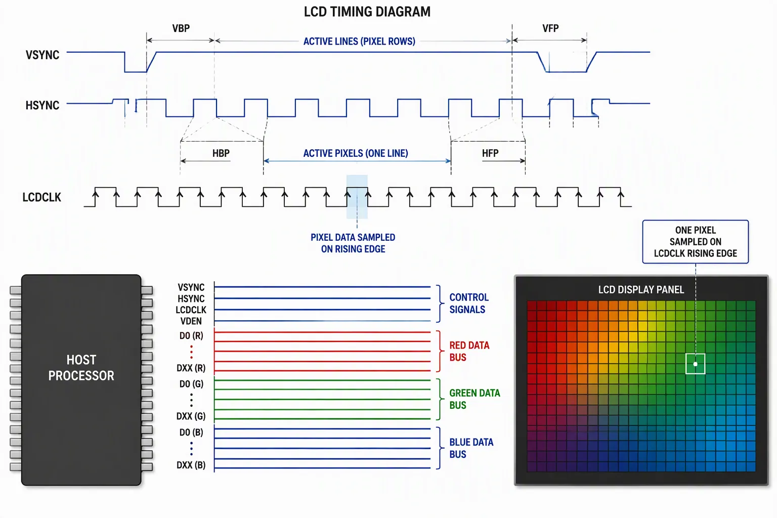
VSYNC, HSYNC, Data Lines, and LCDCLK
Four signal groups carry every frame across a parallel RGB link. Each one has a distinct job, and the panel fails to lock if any of them drifts.
сигнал | Определение | Роли |
|---|---|---|
КАДРЫ | Вертикальная синхронизация | Resets the start of a new frame; no image data travels during the VSYNC pulse |
СТРОК | Горизонтальная синхронизация | Resets the next row; the RGB gray-level data for one row must arrive between two HSYNC pulses |
Data lines (D0…DXX) | Parallel RGB data, one line per bit | Carry the gray-level color data for each pixel and row |
LCDCLK | LCD clock, pixel frequency | Synchronizes gray-level data; the TFT drives one pixel per clock, so its length follows the column count of the resolution |
VDEN | Данные позволяют | Tells the panel whether the RGB signals are valid |
The data lines split into three groups: blue LSB to MSB, green LSB to MSB, and red LSB to MSB. Each group carries the color depth for its channel. LCDCLK sets the pixel pace, and every data line is sampled on its edge. VSYNC and HSYNC act as reset pulses for the frame and the row. VDEN adds a validity flag, so the panel ignores data outside the active window. This handshake gives the host tight control over what the display module captures and when. The interface between the host and the panel depends on all four groups staying in step.
Frame and Line Timing Parameters
Blank intervals surround each synchronization pulse, and these intervals define the timing budget. On the horizontal axis, HBP (horizontal back porch) sits after the HSYNC pulse and before the first active pixel. HFP (horizontal front porch) follows the last active pixel and precedes the next HSYNC pulse. The HSYNC pulse width itself is a separate parameter. On the vertical axis, VBP (vertical back porch) follows the VSYNC pulse before the first active line, and VFP (vertical front porch) follows the last active line before the next VSYNC pulse. The VSYNC pulse width is set independently. A pulse that is too narrow can fail to reset the panel, and a pulse that is too wide eats into active time.
These parameters give you direct control over panel lock and image placement. Total line time equals the active pixels plus HBP, HFP, and the HSYNC pulse width. Total frame time equals the active lines plus VBP, VFP, and the VSYNC pulse width. The refresh rate follows from the total frame time: refresh rate = 1 / total frame time. A longer porch buys the panel more settling time, and a shorter porch raises the refresh rate at the same clock. You must match every value to the panel datasheet, because the display controller and the panel driver share this timing contract. Get one porch wrong, and the image shifts or tears.
The control logic inside the driver counts pixels and lines against these parameters. Each HSYNC pulse resets the column counter, and each VSYNC pulse resets the row counter. That counting scheme keeps the signal path aligned frame after frame and gives the driver precise timing control. A stable timing set also protects the panel from partial-frame writes, which show up as flicker or banding. Log the timing values in your bring-up notes, and compare them against the datasheet on every board revision.
Timing Example: 480×272
Calculating Line and Frame Timing
Возьмем 480 × 272 panel running at 16 bpp. The register set stores each display size as a value minus one, so HOZVAL holds 479 and LINEVAL holds 271. The porches and pulses come from the same register block: HBP = 2, HFP = 2, HSYNC pulse width = 41, VBP = 2, VFP = 2, and VSYNC pulse width = 10.
Add the horizontal terms to get the line length in pixel clocks: 480 active pixels + 2 + 2 + 41 = 525 clocks per line. Add the vertical terms to get the frame length in lines: 272 active lines + 2 + 2 + 10 = 286 lines per frame. Multiply the two totals, and one frame needs 150,150 pixel clocks. The pixel clock itself comes from the bus clock divided by twice the clock divider plus one, so the divider setting sets the pace for the whole signal chain.
Deriving the Refresh Rate
The refresh rate follows from the pixel clock divided by the clocks in one frame. At a pixel clock of 7.83 MHz, divide by 150,150, and you land near 52.1 Hz.
That figure sits within a typical panel rating, so treat it as a check on your register math. Confirm the pixel clock against the panel datasheet before you commit the timing. A wrong clock value throws off every porch and pulse downstream. Log the line total, the frame total, and the resulting refresh rate in your bring-up notes, then compare them on each board revision. This habit keeps the control path honest and catches timing drift early. The control logic inside the driver counts pixels and lines against these same values, so a clean calculation gives you a stable display and a signal the panel can lock to.
LED Driving Control Workflow
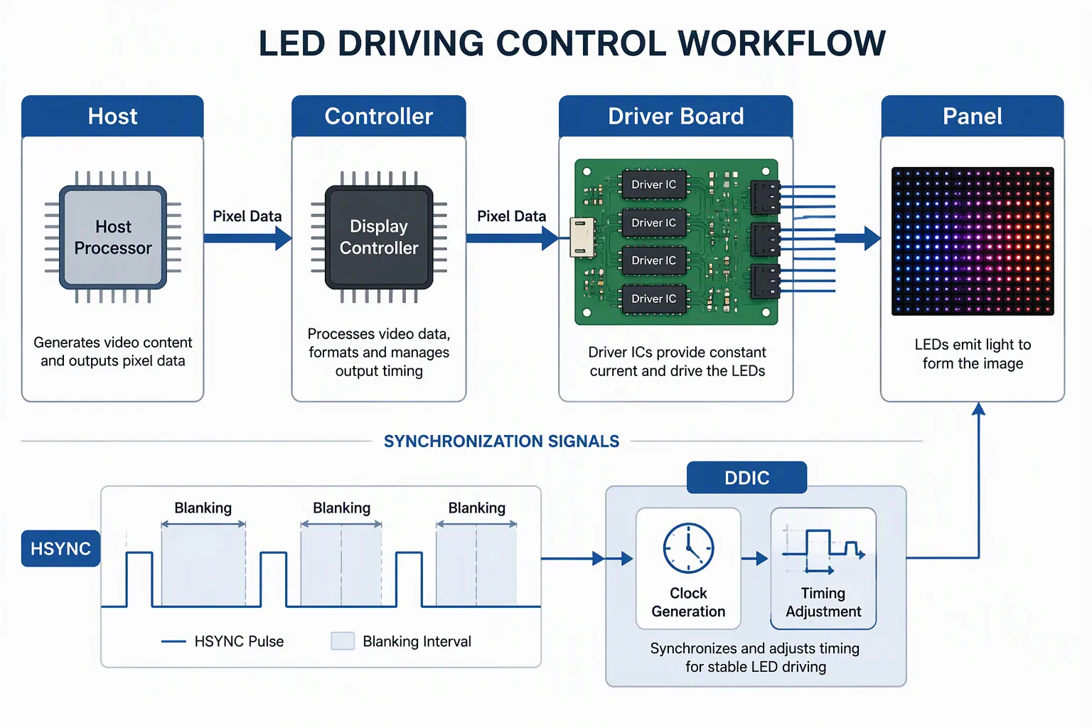
The Data-to-Light Signal Chain
The led driving control workflow starts at the host processor. Your host renders a frame and hands it to the display controller. That controller formats the pixels and pushes them across the interface to the driver board. The driver board holds the driver ics that latch each pixel value. From there, the data moves to the panel, where each pixel electrode receives its analog voltage. Light follows.
This display signal chain has four stages: host, controller, driver board, and panel. Each stage passes the frame forward with its own clock. The host sets the image content. The controller sets the timing. The driver ics set the voltage. The panel sets the light. A break at any stage stops the whole led display system.
Brightness control adds one more layer. In a backlit LCD, led drivers set the light level behind the glass. In a true LED matrix, led drivers set each pixel directly. Either way, the driving principle of an led screen stays the same: current in, light out. Constant-current driver ics hold that current steady, and pwm dims it without color shift. The lcd/led display driver ties these stages into one path from bits to photons.
Synchronization Between Driver and Interface
Frame-by-frame lock depends on dedicated timing control and synchronization circuitry inside the DDIC. Advanced clock generation circuits align the driver with the incoming frame timing. Timing adjustment techniques then compensate for differences in display size and resolution, so frames stay synchronized. An integrated timing controller coordinates pixel activation and deactivation, which keeps the refresh rate stable and frame transitions smooth.
The sync pulses and blanking intervals do the real work. Each one gives the DDIC a fixed reference point.
Временной параметр | Role in Frame Synchronization |
|---|---|
HSYNC (horizontal sync pulse width) | Marks the start and end of each horizontal line so the DDIC aligns pixel data line by line |
HBP (horizontal back porch) | Blanking interval after HSYNC that allows internal processing before active pixels |
HFP (horizontal front porch) | Blanking interval before the next HSYNC that completes the horizontal period |
VSYNC (vertical sync pulse width) | Marks the start and end of each frame so the DDIC aligns frame by frame |
VBP (vertical back porch) | Blanking lines after VSYNC for internal processing before active lines |
VFP (vertical front porch) | Blanking lines before the next VSYNC that complete the vertical period |
These parameters define the total clock cycles and lines per frame, not just the visible pixels. The pixel clock derives from total horizontal period times total vertical period times frame rate. The DDIC uses these sync and blanking intervals to lock onto each interface frame. Your control system must match every value to the panel datasheet. One wrong porch breaks the lock, and the image tears. Constant current driver ics and the timing block work as one unit here. Pulse width modulation handles dimming, and the sync path handles placement. Keep both in step, and every frame lands where it should.
Driver Design and LED Driver Technology
Key Driver Design Considerations
A display driver IC sits between your MPU or MCU and the glass. It plays three roles: translation, interface, and control. On translation, the chip converts incoming image data into precisely sequenced electrical waveforms for the source, gate, segment, and common driver functions. The panel turns those waveforms into luminance and color. This work demands robust signaling integrity across long interconnect paths and consistent behavior over temperature and operating voltage ranges.
On interface, the panel connection method shapes your driver design. You pick among three packaging routes, and each one trades cost against bezel size.
Способ упаковки | Монтаж и маршрутизация | Компромисс |
|---|---|---|
COG | Driver mounted directly on glass | Lowest cost, simplest design, larger visible border |
КОФ | Driver on flexible film folded behind the panel | Balanced cost, smaller front border |
COP | Driver region hidden behind the active area on a flexible substrate | Premium form factor, narrowest bezel |
On control, finer pixel structures demand tighter timing alignment. Small deviations cause visible artifacts, inconsistent luminance, or reduced uniformity. Your driver ics must generate, sequence, and synchronize signals with the panel scan operations. Power efficiency matters too. Smarter drive management cuts energy during active updates and brightness transitions without harming signal quality.
Selecting Driver Technology for the Application
Accurate pixel control ensures every pixel receives the correct voltage or current at the right time. You get consistent brightness, accurate colors, and smooth motion. Higher resolution and refresh rates make precise control even more critical. Large OLED panels add another burden: the chip must compensate for longer signal paths, timing variations, and TFT characteristic differences using calibration data and voltage compensation.
Your choice of led driver technology follows the application. Backlit LCDs need led drivers that set overall light output, while true LED matrix panels need led drivers that set every pixel. Constant-current driver ics hold the set current steady, and their constant current accuracy stays under 0.1%. A pwm scheme dims the light without color shift. The same pwm path supports brightness control across the control system. Build your control logic around over-temperature and over-current shutdown, and the led driver protects itself. A well-chosen driver circuit and a matched control system keep the lcd/led display driver predictable from prototype to volume production.
The interface supplies synchronized data and timing. The driver ics convert that data into per-pixel analog voltages. Timing parameters, driver design, and led driver technology combine to form one complete frame. Your led drivers set current, pwm handles brightness control, and the refresh rate follows from total frame time.
You now see why this partnership matters. A wrong porch breaks the signal lock. A weak led driver circuit adds flicker. Good control starts with the datasheet. Debug one stage at a time, and your display will lock frame after frame. Driver ics, pwm dimming, and led drivers all share one timing contract. Learn it well, and every future panel becomes easier to bring up.
FAQ
What does the driver IC do that the interface cannot?
The interface only moves bits and timing pulses. The driver IC latches each pixel value and converts it into an analog voltage on the pixel electrode. Without that translation step, the data never becomes light. You need both halves working together for any frame to appear.
Why do LED drivers regulate current instead of voltage?
Forward voltage falls as the junction heats up. A resistor circuit then lets current climb, and the extra heat repeats the loop. Constant-current driver ICs hold the set current steady, with accuracy under 0.1%. That stability protects the LED and keeps brightness repeatable across temperature and aging.
When should you choose MIPI DSI over parallel RGB?
Pick MIPI DSI when bandwidth and pin count matter. Four lanes at 2.5 Gbps each deliver roughly 10 Gbps, enough for 4K at 60 Hz. Parallel RGB suits medium panels with direct timing. Small instrument clusters and healthcare devices often run on I2C or SPI instead.
What happens if a porch or pulse width is wrong?
The panel loses its lock on the incoming frame. A narrow sync pulse may fail to reset the panel, and a wide one eats active time. The image then shifts, tears, or flickers. Match every timing value to the panel datasheet, and log them for each board revision.
How do you verify your timing math during bring-up?
Add the active pixels to HBP, HFP, and the HSYNC pulse width to get clocks per line. Add the active lines to VBP, VFP, and the VSYNC pulse width to get lines per frame. Multiply both totals, then divide the pixel clock by that product to check the refresh rate. This control check catches register errors early.