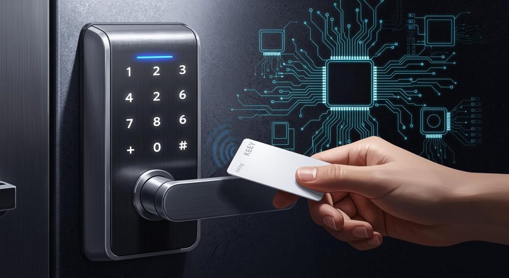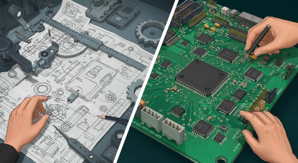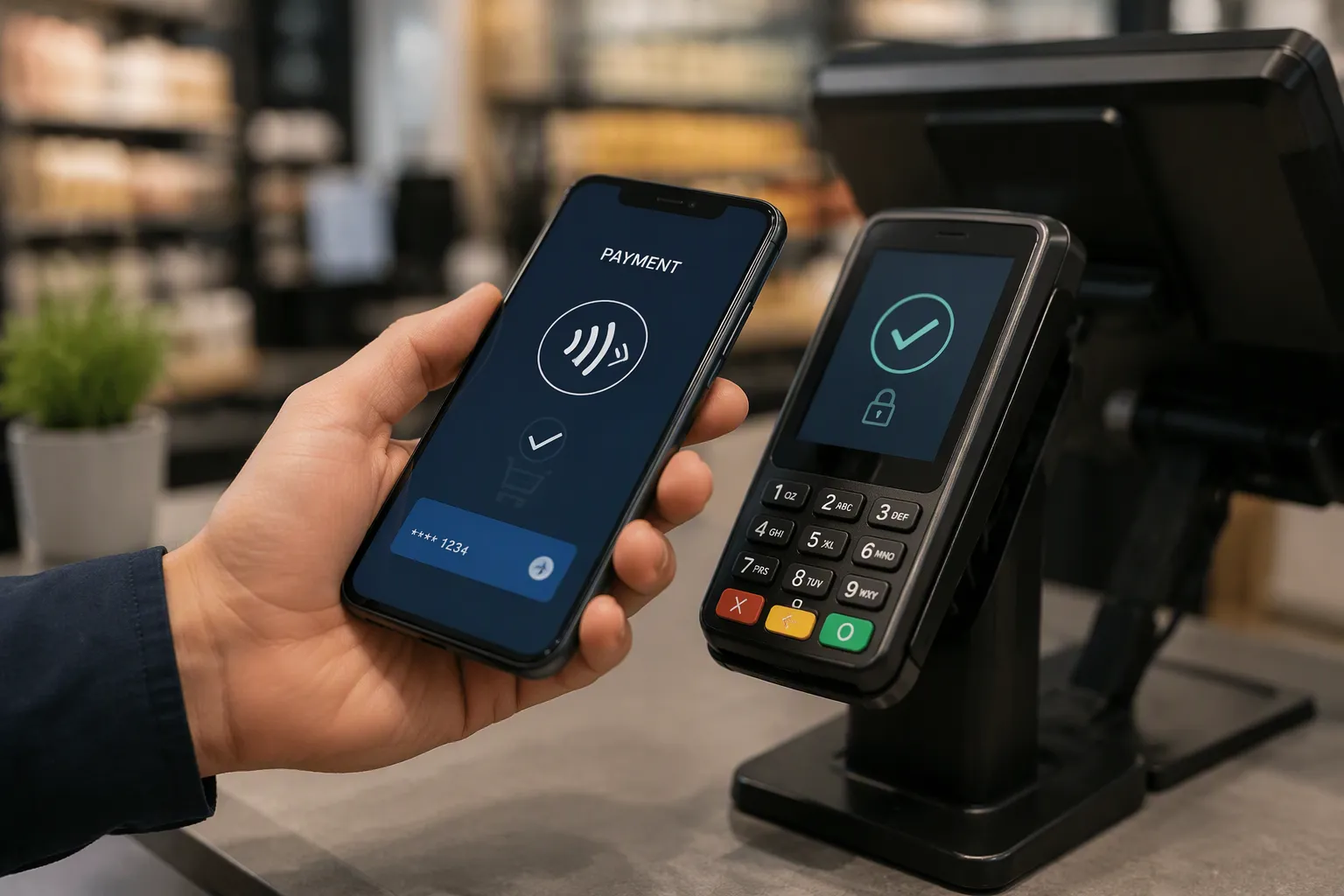
Near field communication is a short-range wireless technology for contactless data exchange. In secure payment solutions, this same radio link moves card data between a terminal and a secure element. The hardware underneath carries the real burden.
This article focuses on board-level design and manufacturing for NFC payment devices. It asks how NFC technology works in payments, what makes it secure at the board level, and which design and DFM constraints matter most.
Hardware engineers and product teams need practical answers, not consumer-level summaries. The sections that follow treat near-field communication as a circuit and layout problem, where antenna geometry, matching, shielding, and tolerances decide whether contactless payments work reliably in the field.
Ringkasan Utama
NFC payments use a 13.56 MHz radio link. The board must work in both reader and card modes.
Tuning the antenna inside the final case is very important. Metal and coatings can change the resonant frequency.
Placing the secure element carefully and shielding it keeps keys safe from probing and side-channel attacks.
Small differences in how a product is made can change how well its antenna works. After coating, tune it again, and check each version you build.
DFM discipline turns early models into dependable contactless payment devices.
NFC and How Does It Work in Payments
Near field communication uses a magnetic field at 13.56 MHz. The way a transaction flows and the mode it runs in both shape the board design. Engineers who understand what is nfc at the circuit level build payment terminals that work more reliably.
The 13.56 MHz Transaction Flow
The NFC interface first listens on the 13.56 MHz channel. A steady carrier wave from an active reader creates an H-field above about 0.185 A/m RMS. When the device senses that field, it may only work in Card Mode. This listen-before-talk rule stops devices from interfering with each other.
A quiet channel lets a reader-capable interface switch into Reader Mode. The board then sends a steady carrier wave for a few milliseconds to start battery-less transponders. After that, the reader runs a polling loop. It pauses with no carrier to reset transponders, applies the carrier to power and start them, sends a polling command in the chosen protocol, then holds the carrier so the response can come back.
This sequence sets the board-level split. Modus pembaca needs the board to create and manage an RF carrier, including field generation, timing, and protocol polling. Card Mode needs the board to sense the field and respond as a transponder. Contactless payment processing depends on both roles working within tight timing windows.
Reader Mode vs. Card Mode
The mode decides controller selection, antenna behavior, and power budget. The table below compares the two roles for nfc payments hardware.
Board-level factor | Reader / Writer Mode | Mode Emulasi Kartu |
|---|---|---|
Pemilihan pengontrol | Reader-capable NFC controller IC over I²C/SPI/UART | Hardware-isolated Secure Element or Host Card Emulation |
Desain antena | Coil geometry, turns, and tuning control read range | Coil must couple to an external reader field; metal detunes it |
Anggaran listrik | Polling interval and RF driver current matter | Power comes from the reader field; low-power state cycling matters |
RF handling | Firmware manages protocol stack and RF timing | Interface handles response timing and field sensing |
Gunakan kasus | Tags, transit cards, labels | Mobile wallet and tokenisation schemes |
A terminal design usually needs a reader-capable controller. A card emulation design centers on the secure element and its isolation. Contactless mobile payments on phones use the card role, while point-of-sale hardware uses the reader role.
Note: The mode choice changes the bill of materials early. Pick the controller before you finalize the antenna.
Protocol Stack and Timing Constraints
The protocol layer sits above the RF carrier. The reader firmware manages device discovery, anti-collision, and command sequencing. The host processor stays free from real-time RF work. This split keeps timing predictable.
NFC technology in payments also depends on EMV timing rules. The reader must finish its polling cycle and hand off data within set windows. A slow host interface can stall the loop. Designers should keep the controller-to-host bus short and free of contention.
Security enters at this layer too. Tokenisation replaces card data with a limited-use token. The secure element stores keys and runs cryptographic operations. The board must protect that element from probing and side-channel access.
Tip: Check field-sensing thresholds and polling timing on the bench before layout freeze.
Antenna Design for NFC in Payments
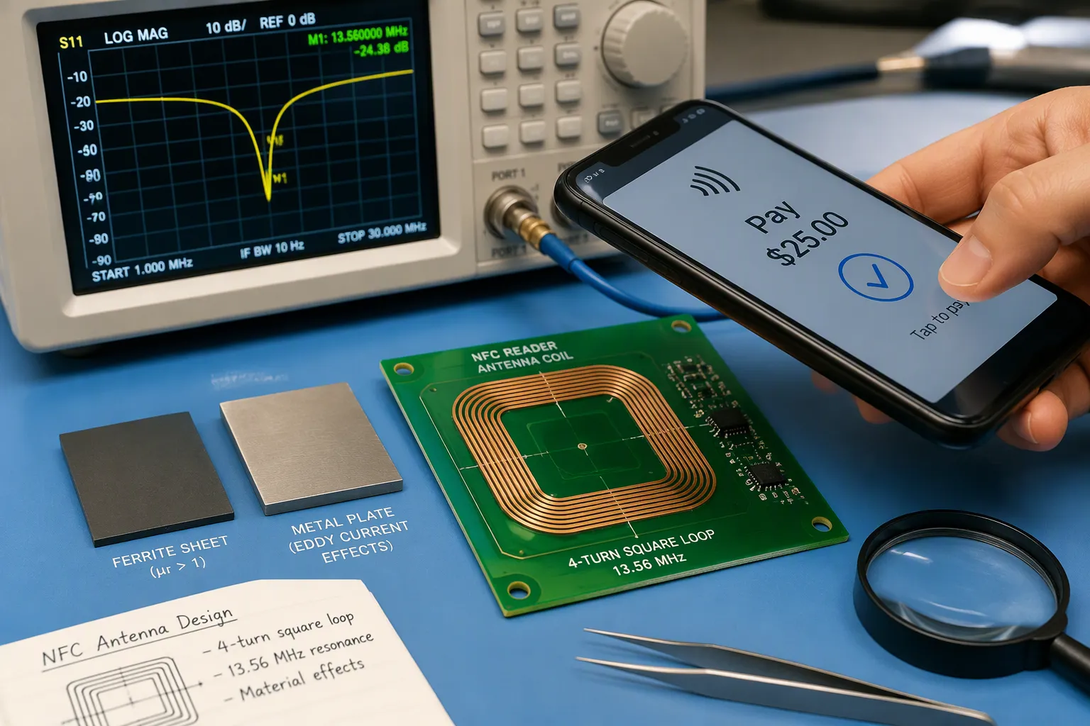
The antenna sets the physical limit on every contactless transaction. A well-tuned coil gives an pembaca NFC room to handle misalignment and metal. A poorly tuned coil fails certification and field tests. The design work splits into loop geometry, matching, and material effects.
Loop Geometry and Matching Networks
Loop size, trace width, spacing, and turn count set the inductance. A typical 4-turn, 40mm × 40mm loop with 0.3mm traces and 0.3mm spacing gives about 1.5–2.5 µH, a range most NFC controllers accept. Turn count changes the value further:
1–3 turns: 0.5–1.5 µH, common for reader antennas with external matching
4–6 turns: 1.5–5 µH, the best range for most NFC applications
7+ turns: higher inductance, but inter-winding capacitance pulls the self-resonant frequency down
The pencocokan jaringan changes the coil impedance to the controller’s target. Series and parallel capacitors set the resonant point at 13.56 MHz. The Q-factor then decides bandwidth. Typical NFC antennas run a Q of 20–40. Higher Q means a more selective tank and a narrower bandwidth. The table below lists common starting values.
Q-faktor | Kondisi Desain |
|---|---|
10 | Matching start value for an NFC reader supporting higher bit rates (212/424/848 kbit/s) |
15 | Matching start value for an NFC reader supporting higher bit rates (212/424 kbit/s) |
20 | Matching start value for a typical NFC reader design |
25 | Matching start value for a typical NFC reader design, limited to 106 kbit/s |
30 | Nominal value for MIFARE Classic communication |
Tip: Tune the matching network inside the final enclosure. Free-air tuning drifts once the housing and battery sit next to the coil.
Ferrite, Metal, and PCB Material Effects
Metal near the coil causes eddy currents. These currents fight the reader field, lower inductance, and raise AC resistance. The resonant frequency shifts upward, away from 13.56 MHz, and the front end sees an impedance mismatch. Read range drops sharply or fails outright.
Ferrite sheets work as magnetic flux concentrators and shields: their high permeability gives field lines a preferred low-reluctance path, concentrating the field outward and minimizing interaction with nearby metals, thereby increasing antenna efficiency, extending range, and reducing power consumption. In contactless payment and access cards, thin flexible ferrite sheets prevent signal degradation when cards are stacked or placed on metal—a phenomenon known as detuning.
The measured effect is large. A coil on a plastic cover read at 78 mm. The same coil on a metal can failed below 1 mm. Adding ferrite brought it back to 30 mm. Ferrite plus repeated impedance matching reached 61 mm. Ferrite alone does not fix detuning. Final matching in the mechanical assembly does.
PCB material matters for tuning stability. FR4 is cost-effective, but its dielectric constant varies between batches and its loss tangent sits near 0.02 at 13.56 MHz. Rogers laminates keep dielectric loss low. Polyimide flex suits bendable designs and shows a lower loss tangent near 0.005. Dielectric thickness, copper thickness, and stack-up consistency all shift capacitance and inductance. Lock the stack-up before final tuning.
Practical Layout Guidelines for NFC Coils
Keep the coil away from ground planes and battery cans. Route no switching traces under the loop. Place the matching components close to the coil pads and keep their ground return short. Check resonance on a vector network analyzer with the unit fully assembled. Re-check every build variant, because a changed housing or battery alters the tuning.
Board-Level Security for Secure Payment Solutions
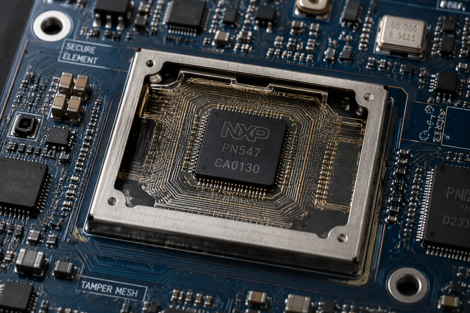
Keamanan di solusi pembayaran yang aman starts on the copper. The protocol protects data while it moves, but the board must protect keys, firmware, and the secure element itself. Product teams should treat this as a layout and manufacturing problem, not a software add-on.
Secure Element Placement and Shielding
Placement decides how hard an attacker must work. Designers should put the elemen aman near the middle of the PCB and surround it with non-critical components. Those parts act as a physical barrier against probing. Sensitive parts also belong away from board edges, where tools reach easily. A protective layer or enclosure adds another step for anyone with physical access.
Electrical isolation matters just as much. The secure element should use its own power and ground connections, separate from the rest of the circuit. Shared rails leak information through side-channel attacks. Connect power and ground pins directly to their planes with little trace exposure to lower EMI risk. Route critical traces on inner layers between ground planes, which gives natural shielding against probing. A continuous ground plane prevents loops and provides low-impedance return paths, with a target of roughly 50 ohms impedance for high-speed signals.
Tip: Ground every shield properly. A floating shield becomes an unintended antenna and makes EMI worse.
A Faraday cage-like structure around the element blocks electromagnetic fields and RF attacks. Metal cans and conductive coatings both work. This shielding supports secure transactions in nfc payments, where an attacker may try to couple energy into the element without touching it.
Tamper Detection and EMVCo/PCI Considerations
Tamper detection turns the board into a sensor. Mesh layers, trip traces, and light or temperature sensors detect opening, drilling, or probing. The controller then erases keys before an attacker can read them. Designers should route mesh traces on inner layers and keep them continuous around the element. A break in the loop must trigger a response within the detection window the product defines.
Certification shapes these choices. EMVCo and PCI standards govern contactless payment processing hardware, and auditors examine physical protection, key storage, and tamper response. The table below compares common protection approaches.
Pendekatan | Board-Level Effect | Pengorbanan |
|---|---|---|
Center placement with surrounding parts | Blocks direct probing | Consumes routing area |
Dedicated power and ground | Limits side-channel leakage | Adds plane splits |
Faraday shielding | Blocks RF coupling | Needs solid grounding |
Tamper mesh on inner layers | Detects intrusion | Raises layer count |
Note: Document every security decision at design freeze. Auditors ask for the rationale, not just the result.
Security as a Manufacturing Concern
Security survives only if production repeats it. Assembly houses must control access to secure boards, track panel serialization, and protect firmware during programming. Conformal coating and potting protect mesh traces from environmental damage that could cause false alarms. Test fixtures should verify tamper loops without leaving probe marks that weaken them.
Tokenization for added security reduces what the board stores, yet encryption keys still live in the element. A mobile wallet transaction passes through the same protected path as a card tap. Teams should treat every contactless build variant as a new security review, because a changed enclosure or shield alters the threat surface. This discipline separates a secure payment method from a device that only claims to be one.
Making Contactless Payments with NFC: DFM Constraints
Manufacturing Trade-Offs and Tolerances
Fabrication tolerances can shift the antenna’s resonant point. Etch variation changes trace width and spacing, which moves inductance away from the tuned value. Dielectric thickness variation alters parasitic capacitance between the coil and nearby copper. A design that tunes cleanly on one panel may drift on the next. Engineers should specify the stack-up and copper weight, then confirm resonance across the full tolerance window rather than at nominal.
Material choice carries its own trade-offs. FR4 keeps cost low, yet its dielectric constant varies between batches and its loss tangent sits near 0.02 at 13.56 MHz. Rogers laminates hold tuning more stably at higher material cost. Polyimide flex suits bendable builds and shows a lower loss tangent near 0.005. The table below compares common options for NFC boards.
Bahan | Stabilitas Penyetelan | Biaya Relatif | Penggunaan Khas |
|---|---|---|---|
FR4 | Moderate; batch variation | Rendah | Rigid terminals |
Rogers | High | High | Tight-tolerance readers |
Polimida fleksibel | Good; low loss | Moderat | Bendable antennas |
Assembly adds further variation. Solder volume on matching capacitors shifts their effective value. Component placement tolerance moves the ground return path. Conformal coating changes the local dielectric environment around the coil.
Tip: Re-tune after coating. The shift is small but measurable.
Practical Guidelines for Product Teams
Teams making contactless payments with NFC should lock the stack-up before final tuning. Freeze the enclosure, battery, and ferrite placement at the same time. Every build variant deserves a fresh resonance check on a vector network analyzer, because a changed housing alters the field.
Avoid routing switching traces under the loop. Keep matching components close to the coil pads. Specify panel serialization so field failures trace back to a lot. For nfc payments, treat the antenna and the secure element as one controlled process, not two.
Note: Document tolerance limits at design freeze. Production repeats what the drawing states.
Secure payment solutions depend on careful board-level work. Antenna design sets how far the reader can reach. Matching and tuning keep resonance at 13.56 MHz for every build. Secure element placement, shielding, and tamper detection keep keys safe from probing. DFM discipline carries all of this into production.
Near-field communication by itself does not make a device trustworthy. Secure nfc hardware depends on engineering and manufacturing trade-offs that teams control at design freeze. Expect closer alignment between nfc and emv certification, along with changing shielding techniques.
Hardware engineers should lock the stack-up, re-tune after coating, and check every variant. That discipline turns contactless prototypes into reliable contactless payments hardware. Careful teams ship secure contactless devices with confidence.
FAQ (Pertanyaan Umum)
What is NFC and why does it matter for payment hardware?
Near-field communication is a short-range radio link at 13.56 MHz. In payments, it moves card data between a terminal and a secure element. Hardware teams should treat it as a circuit and layout problem, not a software feature.
How do engineers keep NFC payments secure at the board level?
Security starts on the copper. Teams should center the secure element, isolate its power and ground, and add tamper mesh on inner layers. Shielding blocks RF coupling. Auditors check these choices against EMVCo and PCI rules.
Which antenna factors most affect contactless payments reliability?
Loop geometry, matching network tuning, and nearby metal decide read range. Engineers should tune inside the final enclosure and re-check every build variant. Ferrite helps with metal, yet final matching still matters.
Note: A coil that reads well in free air can fail once the battery and housing sit next to it.
How does a mobile wallet transaction differ from a card tap at the board level?
Both use the same 13.56 MHz field and card emulation role. A phone runs a mobile wallet through its secure element. A card tap uses a passive coil. The reader side handles both the same way.