При проектировании печатной платы GPS вы контролируете, насколько хорошо работает ваш GPS-приемник. Качественное проектирование печатной платы GPS повышает точность и обеспечивает надежность устройства. Ошибки могут привести к таким проблемам, как увеличение длины дорожек, усиление шума и даже короткие замыкания. Эти проблемы могут негативно сказаться на работе GPS-приемника. К распространенным проблемам относятся:
Увеличение длины трасс , ослабляющее целостность сигнала.
Перекрывающиеся детали, создающие шум и тепло.
Небольшие зазоры между деталями, вызывающие короткое замыкание.
Тщательное планирование поможет избежать этих проблем и создать надежное GPS-устройство.
Основные выводы
Правильное размещение антенны на верхнем слое печатной платы повышает качество и точность приема сигнала GPS.
Используйте методы согласования импеданса для обеспечения плавной передачи сигнала от антенны к приемнику, что позволит уменьшить потери сигнала.
Чтобы избежать распространенных ошибок проектирования и улучшить работу GPS, следуйте рекомендациям, указанным в технической документации, при оформлении макета.
Внедрите маршрутизацию с контролируемым импедансом для поддержания целостности сигнала и снижения электромагнитных помех.
Для обеспечения надежной работы GPS-навигатора используйте высококачественные материалы и соблюдайте жесткие производственные допуски.
Размещение GPS-антенны

Выбор места для GPS-антенны играет ключевую роль в проектировании печатной платы GPS. Расположение антенны влияет на точность и производительность GPS. Для надежной навигации вашему устройству необходим четкий сигнал. Тщательное размещение помогает избежать помех и потери сигнала.
Позиционирование верхнего слоя
Антенну GPS следует размещать на верхнем слое печатной платы. Такое положение обеспечивает антенне свободный путь для приема сигналов со спутников. Необходимо избегать препятствий, блокирующих или ослабляющих сигнал. Антенну следует размещать подальше от шумных компонентов, таких как процессоры и силовые цепи. Также необходимо обеспечить достаточное пространство вокруг антенны. Это пространство способствует лучшему излучению энергии антенной и повышает ее производительность.
Совет: Разместите GPS-антенну ближе к краю печатной платы. Это уменьшит помехи и усилит сигнал.
Согласование импедансов для повышения производительности
Согласование импедансов помогает максимизировать передачу мощности и минимизировать отражение сигнала. Необходимо, чтобы сигнал беспрепятственно распространялся от антенны к GPS-приемнику. Для этого можно использовать согласующие цепи, такие как L-образные, π-образные или T-образные. Эти цепи помогают регулировать импеданс между антенной и дорожками печатной платы. Также необходимо согласовать характеристический импеданс дорожек с импедансом системы. Этот шаг уменьшает потери сигнала и улучшает конструкцию печатной платы GPS.
Для соединения антенны и приемника используйте согласующие цепи.
Согласуйте импеданс трассы с импедансом системы.
Избегайте резких изгибов дорожек, чтобы сохранить целостность сигнала.
Выполнение этих шагов улучшит работу GPS. Сигнал останется сильным и чистым, что обеспечит точную навигацию.
Оформление в соответствии с рекомендациями, указанными в техническом описании.
При проектировании GPS-антенны всегда следует руководствоваться рекомендациями, указанными в техническом описании. В техническом описании содержится важная информация о расстоянии между элементами, ширине дорожек и заземлении. Чтобы избежать распространенных ошибок, следует проверить техническое описание перед проектированием печатной платы GPS. Антенну следует размещать вдали от металлических деталей и больших заземляющих плоскостей. Для печатной платы следует использовать материалы, рекомендованные для поддержки сигналов GNSS.
Примечание: Данная спецификация поможет вам выбрать правильную компоновку для вашей печатной платы GPS. Следуя этим инструкциям, вы добьетесь большей точности и производительности.
Правильное размещение антенны закладывает прочную основу для GPS-устройств. Это позволяет избежать потери сигнала и помех, а также обеспечивает надежную навигацию и стабильную работу устройства.
Структура слоев в проектировании печатных плат GPS
Многослойная конфигурация
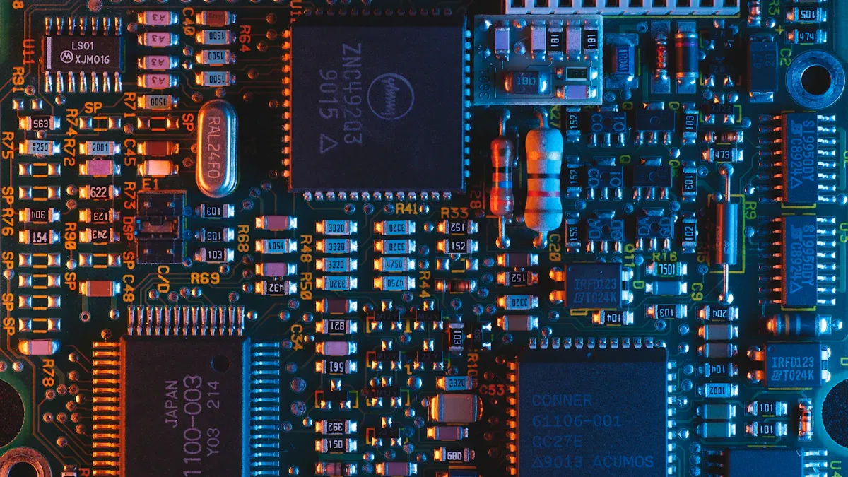
Многослойная структура печатной платы GPS обеспечивает прочную основу для проектирования GPS-платы. Наличие нескольких слоев помогает управлять сигнальными путями и уменьшать помехи. Вы повышаете производительность и точность GPS, отделяя высокоскоростные трассы от силовых и заземляющих плоскостей. Антенна GPS располагается на верхнем слое для обеспечения четких навигационных сигналов. Типичная структура печатной платы для высокопроизводительной GPS-системы представлена в таблице ниже:
Номер слоя | Описание |
|---|---|
1 | Высокоскоростные сигнальные трассы и компоненты |
2 | Наземная плоскость |
3 | Силовая плоскость (например, 3.3 В) |
4 | Силовая плоскость (например, 5 В) |
5 | Наземная плоскость |
6 | Дополнительные трассировки сигналов или низкоскоростной ввод-вывод |
Эта структура используется для обеспечения чистоты сигналов и снижения уровня шума. Она также упрощает маршрутизацию сложных GPS-цепей.
Настройка плоскости заземления и питания
Для защиты чувствительных сигналов GPS вы устанавливаете заземляющую и силовую плоскости. Заземляющие плоскости располагаются близко к сигнальным слоям, чтобы экранировать их от помех. Для предотвращения перекрестных помех используются отдельные силовые плоскости для разных напряжений. Заземляющая плоскость должна быть непрерывной под антенной GPS и сигнальными дорожками. Этот шаг помогает поддерживать целостность сигнала и повышать производительность GPS.
Совет: Избегайте разделения плоскостей заземления. Они должны оставаться сплошными для обеспечения надежной навигации и работы GNSS.
Выбор диэлектрического материала
Для минимизации потерь сигнала на печатной плате вы выбираете подходящий диэлектрический материал. Для высокоскоростных GPS-сигналов вы выбираете материалы с низкой диэлектрической постоянной. Вы повышаете производительность и уменьшаете перекрестные помехи между дорожками. Преимущества этих материалов вы можете увидеть в таблице ниже:
Преимущества | Описание |
|---|---|
Высокоскоростное распространение сигнала | Снижение потерь благодаря низкой диэлектрической постоянной. |
Уменьшение перекрестных помех | Минимизирует помехи между дорожками и переходными отверстиями. |
Ограничения емкостной связи | Уменьшает сложность схемы и повышает производительность. |
Несоответствие длин трасс | Снижает негативные последствия в параллельных сетях. |
Для проектирования печатных плат GPS вы выбираете такие материалы, как Rogers 4350B, RT Duroid 5880 и Isola-I speed . Эти материалы помогают добиться высокого качества сигнала и надежной точности GPS.
При разработке печатной платы GPS, обеспечивающей надежную навигацию и работу GNSS, вы уделяете особое внимание структуре слоев. Вы защищаете сигналы, снижаете уровень шума и обеспечиваете надежность устройства.
Целостность сигнала и радиочастотные характеристики
Для достижения максимальной точности и производительности необходимо защищать сигналы GPS от шума и помех. Качественная разработка печатной платы GPS помогает поддерживать чистоту и устойчивость сигнала. Для улучшения целостности сигнала и обеспечения надежной навигации можно использовать несколько методов.
Снижение электромагнитных помех и перекрестных помех
Электромагнитные помехи (ЭМП) и перекрестные помехи могут ослаблять сигналы GPS и снижать точность. Для уменьшения ЭМП и перекрестных помех на печатной плате можно предпринять следующие шаги :
Разместите все внешние соединения на одном краю печатной платы. Такая схема помогает контролировать шум и обеспечивает упорядоченность сигналов.
Избегайте прокладки высокоскоростных дорожек вблизи края. Это обеспечит надежное заземление и предотвратит нежелательные помехи.
Если между разъемами проходят высокоскоростные цепи, установите печатную плату на металлический корпус. Этот метод предотвращает наведенное напряжение и защищает GPS-антенну.
Проверьте наличие трасс ввода-вывода вблизи высокоскоростных трасс. Это предотвратит перекрестные помехи еще до их возникновения.
Заземлённые радиаторы с низкоимпедансным соединением. Это уменьшает электрическую связь и обеспечивает чистоту сигналов GPS.
Выполнение этих шагов позволит улучшить производительность GPS и повысить надежность вашего устройства.
Технологии волноводов и обратного сверления
Для повышения радиочастотных характеристик GPS-платы можно использовать волноводы и обратное сверление. Обратное сверление удаляет неиспользуемые участки переходных отверстий, что помогает уменьшить отражение сигнала и задержку. Этот метод лучше всего работает на многослойных печатных платах с высокочастотными GPS-сигналами. Например, обратное сверление может уменьшить задержку сигнала с 12 пс/дюйм до 5 пс/дюйм при частоте сигнала выше 15 ГГц. Вы получаете более быстрые и чистые GPS-сигналы, что приводит к повышению точности навигации и GNSS. Для однослойных или двухслойных плат обратное сверление может не дать достаточной выгоды за счет снижения затрат.
Экранирование и развязка
Экранирование и развязка защищают схемы GPS от шума и помех. Эти методы помогут обеспечить надежность вашей печатной платы GPS:
Для блокировки внешнего шума используйте металлические корпуса и заземляющие пластины .
Изолируйте критически важные цепи с помощью экранирующих элементов на уровне печатной платы и токопроводящих корпусов.
Предотвратите распространение шума, используя методы шумоизоляции.
Для высокочастотной фильтрации выбирайте проходные или отводные конденсаторы с низкой индуктивностью выводов.
В цепях с высокими пульсациями или изменениями напряжения используйте твердотельные конденсаторы.
Эти шаги помогут вам поддерживать качество сигнала и улучшить работу GPS. Вы обеспечите надежную навигацию и стабильную работу GNSS, защитив GPS-антенну от помех.
Стратегии маршрутизации для печатной платы GPS
Маршрутизация с контролируемым импедансом
Использование трассировки с контролируемым импедансом повышает производительность печатной платы GPS. Следуя этим рекомендациям, вы обеспечиваете чистоту и мощность сигнала:
При высокоскоростной трассировке необходимо поддерживать постоянную опорную плоскость . Этот шаг улучшает обратный путь сигнала и предотвращает появление шума.
Избегайте прокладки трасс через разделенные плоскости. Обратный путь сигнала не сможет следовать по трассе, что приводит к электромагнитным помехам и ухудшению работы GPS.
Соблюдайте надлежащую ширину и расстояние между дорожками. Используйте правило 3W, согласно которому ширина заземляющей плоскости должна быть как минимум в три раза больше ширины дорожки с каждой стороны.
Согласуйте длины трасс для дифференциальных пар. Это позволит минимизировать несоответствия задержки распространения и обеспечить точность сигналов GPS.
Выполнение этих шагов обеспечит надежную навигацию и стабильную работу GNSS.
Оптимизация длины трассы
Оптимизация длины дорожек на печатной плате повышает точность GPS. Короткие дорожки помогают сигналам распространяться быстрее и уменьшают количество ошибок. Вы поддерживаете высокую целостность сигнала, что улучшает точность синхронизации и позиционирования в системах GPS. Вы также повышаете надежность вашего устройства. Вы предотвращаете неожиданные сбои в системах, зависящих от сигналов GPS. Вы повышаете эффективность системы, поскольку уменьшаете необходимость повторной передачи сигнала и снижаете количество ошибок.
Совет: Старайтесь, чтобы маршруты были как можно короче и прямее. Это поможет вашей GPS-антенне передавать четкий сигнал для точной навигации.
Трассы передачи сигналов высокой плотности
При прокладке высокоплотных сигнальных трактов на плате GPS вы сталкиваетесь с трудностями. Для их преодоления можно использовать следующие стратегии:
Провода должны быть короткими и прямыми. Это уменьшит количество ошибок и бликов.
Передавайте высокоскоростные сигналы по твердой заземляющей плоскости. При этом сохраняется целостность сигнала.
Увеличьте расстояние между трассами. Это позволит минимизировать перекрестные помехи.
Согласуйте длины трасс для дифференциальных пар. Это позволит избежать искажений и сохранить точность сигналов GPS.
Избегайте прокладки высокоскоростных сигналов вблизи силовых установок. Это предотвратит помехи.
Используя эти стратегии маршрутизации, вы создаёте печатную плату, обеспечивающую высокую производительность GPS и надёжную навигацию.
Производство печатных плат для GPS с улучшенными характеристиками.
Выбор материалов и допусков
Для обеспечения высокой производительности GPS необходимо правильно выбрать материалы. Выбор материала влияет на качество сигнала и надежность. Некоторые материалы лучше подходят для высокочастотных приложений GPS. Основные варианты представлены в таблице ниже :
Тип материала | Ключевые свойства | Лучшие варианты использования |
|---|---|---|
Высокая Tg FR-4 | Высокая температура стеклования, умеренная диэлектрическая постоянная | Автомобильные GPS-навигаторы потребительского класса |
Ламинаты на основе ПТФЭ | Низкая диэлектрическая постоянная, очень низкие потери | Высокочастотные GPS-системы и радиолокационные системы |
Материалы, наполненные керамикой | Низкая диэлектрическая постоянная, высокая теплопроводность | Аэрокосмические и военные навигационные системы |
Polyimide | Отличная термостойкость, низкое расширение | Морские или космические навигационные системы |
Также следует обратить внимание на производственные допуски. Жесткие допуски помогают обеспечить точность прохождения сигнала. Этот шаг способствует стабильной работе печатной платы GPS.
Проектирование с учетом технологичности производства и тестирование
Вы повысите эффективность производства печатных плат, используя лучшие практики проектирования с учетом технологичности изготовления (DFM). Начинайте применять DFM на ранних этапах проектирования. Проверяйте свой проект на каждом этапе, чтобы избежать дорогостоящих ошибок. Следуйте этим советам:
Проверьте схему, размещение компонентов и трассировку на наличие ошибок.
Оставляйте достаточное расстояние между отверстиями для сверления и медными дорожками.
Используйте правильные пропорции для отверстий и толщины платы.
Перед окончательным утверждением проведите анализ DFM (проектирование с учетом технологичности конструкции).
Эти шаги помогут вам снизить затраты, повысить надежность и ускорить вывод продукции на рынок . Также необходимо протестировать плату GPS перед массовым производством. Важные тесты включают :
Тест при включении
тест сигнала GNSS
Проверка подключения антенны
Испытание на циклическое изменение температуры
Вибрационный тест
Финальный функциональный тест
Устройства для использования на открытом воздухе и мобильные устройства требуют дополнительной проверки. Перед массовым запуском необходимо протестировать устройство на предмет перепадов температуры, вибрации, работы батареи и стабильности беспроводной связи.
Гарантия качества
Для обеспечения надежности печатных плат GPS необходимо использовать строгие методы контроля качества. Применяйте как ручные, так и автоматизированные проверки. В таблице ниже приведены распространенные методы проверки качества :
Метод тестирования | Описание |
|---|---|
Внутрисхемное тестирование (ICT) | Проверяет цепи на наличие обрывов или коротких замыканий. |
Тест летающего зонда | Обнаруживает неплотные соединения без питания. |
Функциональный тест | Подтверждает, что печатная плата работает должным образом. |
Автоматизированный оптический контроль | Использует камеры для поиска недостающих деталей или проблем с пайкой. |
Рентгеновское обследование | Проверяет печатную плату на наличие скрытых коротких замыканий или повреждений. |
Электрические испытания | Измеряет выходные сигналы для проверки работоспособности. |
Визуальный осмотр | Выявляет физические повреждения, которые могут негативно повлиять на производительность. |
Также следует отслеживать компоненты и этапы сборки. Такая прослеживаемость помогает быстро находить и устранять проблемы. Сочетание этих этапов с надежной интеграцией GNSS обеспечивает более высокую точность позиционирования и более высокий уровень надежности сигнала . Ваша плата GPS будет хорошо работать даже в сложных условиях.
Оптимальная производительность GPS достигается за счет тщательного размещения антенны, целостности сигнала и аккуратного изготовления. Следуйте рекомендациям, указанным в технической документации, при выборе материалов, предотвращающих коррозию и электрические проблемы. Используйте моделирование и тестирование для проверки вашей конструкции. Последние достижения , такие как интеграция антенн и улучшенное экранирование, помогают создавать надежные GPS-устройства. Отраслевые стандарты, такие как ISO 9001 и ISO 9100, гарантируют качество и точность. Постоянно совершенствуйте свои навыки и уделяйте внимание каждой детали для достижения наилучших результатов.
Стандарт | Цель | Влияние на печатные платы GPS |
|---|---|---|
стандартами качества ISO 9001 | Система контроля качества | Обеспечивает надежность и точность |
стандартами качества ISO 9100 | Управление качеством в аэрокосмической отрасли | Поддерживает высокие стандарты |
FAQ
Какой фактор наиболее важен для производительности печатной платы GPS?
Размещение антенны имеет первостепенное значение. Антенну следует размещать на верхнем слое, вдали от источников помех. Этот шаг поможет получить чистый сигнал и повысить точность GPS.
Как уменьшить уровень шума на плате GPS-навигатора?
Вы можете:
Используйте твердые поверхности земли.
Не допускайте появления коротких следов.
Необходимо обеспечить экранирование чувствительных цепей.
Эти шаги помогут блокировать помехи и поддерживать чистоту сигнала.
Какие материалы лучше всего подходят для высокочастотных печатных плат GPS?
Материал | Польза |
|---|---|
Ламинаты ПТФЭ | Низкая потеря сигнала |
С керамическим наполнителем | Высокая термостойкость |
Высокая Tg FR-4 | Подходит для большинства применений |
Материалы следует выбирать в зависимости от потребностей вашего устройства.
Почему необходимо следовать указаниям, приведенным в технической документации?
Наилучшие результаты достигаются при соблюдении правил, указанных в технической документации. Эти руководства показывают правильную ширину, расстояние и расположение трасс. Вы избежите ошибок и повысите надежность GPS-сигнала.