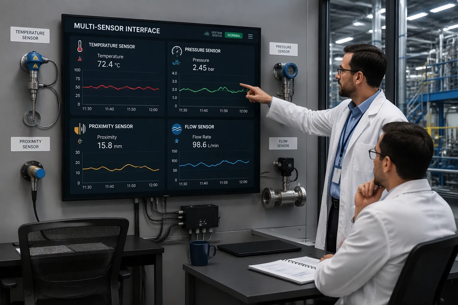
Picture a single machine controller on a factory floor. It must read temperature, pressure, position, and flow at the same time. Each sensor speaks a different electrical language. Some deliver tiny analog voltages. Others send fast digital pulses. Multi-industrial sensor interface design solves this mismatch on one shared platform. Get it wrong, and you risk unreliable readings, degraded signal integrity, slow control loops, safety gaps, and higher cost. You face a real tension here. The signals are wildly heterogeneous, yet the board is one. That conflict shapes every decision you make.
الوجبات السريعة الرئيسية
Match each sensor’s signal to the right conditioning circuit. Amplify weak signals and filter noise early.
Use mixed-signal ICs to shrink board space and change settings in software. This saves time and money.
Keep analog and digital parts separate on the board. Use one solid ground plane and route signals carefully.
Test your board with real-world noise and temperature changes. Calibrate each channel to fix errors.
Plan for future upgrades. Add spare computing power and use reconfigurable interfaces for new sensors.
Architecting Multi-Sensor Interfaces
Every multi-industrial sensor interface design starts with one question: where does the intelligence live? Most industrial boards center it on one controller. That choice shapes your sensor interface design from the first schematic.
Microcontroller-Centric Architecture
A single microcontroller reads multiple sensors through its peripherals and an external analog front end. You get one clock domain, one firmware image, and one place to timestamp sensor data acquisition. This structure keeps a data acquisition pcb compact and predictable. It also simplifies debugging in industrial automation projects, because every reading passes through code you control.
Universal And Reconfigurable Interfaces
Universal interfaces for industrial sensors let one board serve many transducer types. A reconfigurable conditioning module built from operational amplifiers with selectable gains does this job. Firmware links the digital blocks into a complete front end. Sensors connect through a 4-line interface: two power lines and up to two signal lines, with an added resistor in some configurations. The design also offers an IEEE 1451.3 plug-and-play output. Think of it as one universal interface that changes shape in firmware. That universal interface covers analog and digital sensors on a single platform.
Sensor Typology | الاعداد |
|---|---|
Conditioned Sensor | التكوين 1 |
Unconditioned Sensor (Wheatstone bridge like) | التكوين 2 |
Current Output Sensor | التكوين 3 |
مستشعر مقاوم | التكوين 4 |
بالسعة الاستشعار | التكوين 5 |
Digital Sensor (Serial interface: RS232/SPI/Microwire) | Configuration 6/7/8 |
A configurable processor enables runtime modification of monitoring behavior without system redesign, adapting to diverse conditions while keeping complexity manageable.
You activate only the signal conditioning circuits each sensor needs. That flexibility suits custom multi-sensor interfaces in industrial WSN and IoT data collection. It also keeps multi-sensor interfaces reusable across product lines.
Latency deserves early attention. Closed-loop control needs deterministic timing, because delay and packet loss destabilize the loop. WISA and WSAN-FA target about 10 ms across up to 120 devices. IO-Link Wireless targets about 5 ms for up to 40 devices in a single hop. Wired paths run faster: a PLC backplane responds in about 1 ms, and a well-designed setup can reach 20–60 µs, with a worst case near 100 µs. Analog filtering adds delay. Budget sensor fusion and mixed-signal timing around these numbers. Good sensor interfaces and a clear sensor interface plan keep that budget honest.
Multi-Industrial Sensor Interface Design Principles
Signal Conditioning Basics
You start every multi-industrial sensor interface design by matching the conditioning chain to each sensor’s output. A thermocouple produces only a few millivolts per degree Celsius, so you amplify that weak signal with an instrumentation amplifier before it reaches the ADC. A pressure sensor built around a Wheatstone bridge needs bridge excitation and differential amplification. Optical sensors demand current-to-voltage conversion. Each path differs, yet the principles stay constant.
تقنية | الهدف | مثال |
|---|---|---|
توسيع | Boost weak signals for ADC readability | Thermocouple at a few mV/°C |
تخفيف | Scale down large voltages | Resistor dividers |
تصفية | Remove noise and interference | Low-pass, band-pass filters |
عزل كهربائي | Block unwanted current while passing data | Optocouplers, isolation amplifiers |
الإشارات التفاضلية | Cancel common-mode noise | Instrumentation amplifiers with high CMRR |
ADC conversion | Convert conditioned analog to digital | دقة 12/16/24 بت |
تعويض درجة الحرارة | Counteract thermal drift | Thermistors, lookup tables |
Calibration and linearization | Align sensor response to reference | Software auto-calibration |
Your analog signal conditioning circuitry must also handle charge output sensors, which need external charge amplifiers, and internally amplified sensors with built-in integrated circuits. These signal conditioning circuits form the backbone of any reliable industrial sensor interface.
Noise Reduction And Grounding
A full ground plane is your most universal solution for mixed-signal sensor interfaces. It provides easy-to-follow return paths and better EMI shielding than a grid. Avoid splitting the ground plane unless absolutely necessary, because splits disrupt return paths and distort high-frequency signals. Route critical signals directly above a continuous ground plane. Routing over gaps can increase inductance.
Separate analog and digital grounds, then connect them at a single point near the power supply entry. This star grounding stops digital switching noise, which can peak at 100 mV or more, from coupling into analog signals with thresholds as low as 10 mV. Use stitching vias spaced at about one-tenth of the wavelength of the highest frequency signal. For a 1 GHz signal, that spacing is roughly 30 mm, and it can cut EMI radiation by up to 10 dB. Place decoupling capacitors close to IC power pins with short ground connections. Combine values like 0.1 µF and 1 µF for wideband noise suppression.
Mixed-Signal Sensor Interface ICs
Reducing System Complexity
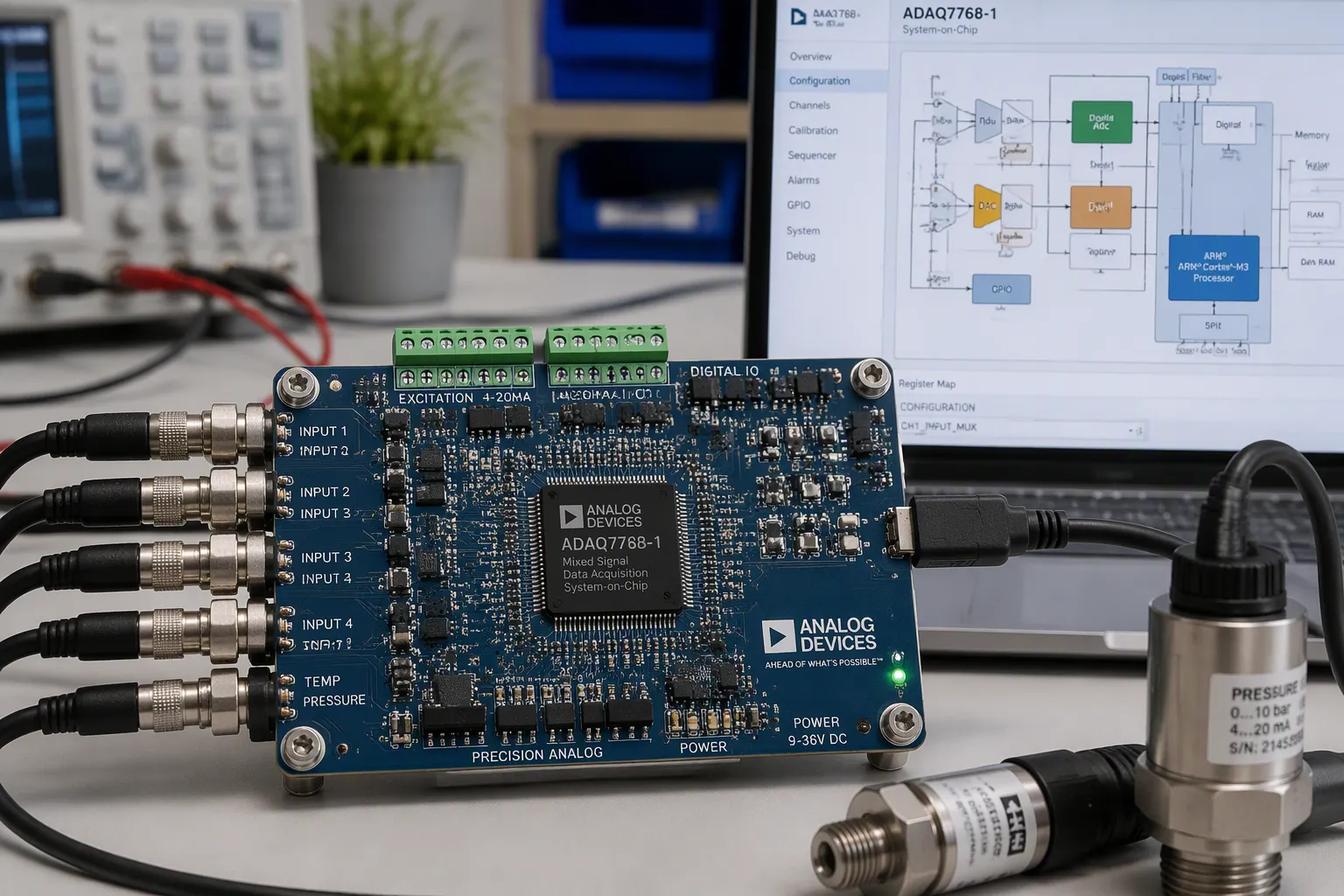
A mixed-signal sensor interface IC puts the analog front end and the digital control on one die. You stop building gain stages, threshold detectors, and filters from separate op-amps and passives. Instead, you configure on-chip blocks in software. This shift changes how you approach multi-industrial sensor interface design.
البعد | Discrete Implementation | Mixed-Signal Sensor Interface IC |
|---|---|---|
الواجهة الأمامية التناظرية | Separate op-amps, comparators, references, passives | Configurable on-chip analog blocks |
الاعداد | Component selection and board layout | Software configuration of internal blocks |
منطقة اللوحة | خط الأساس | توفير يصل إلى 90% versus discrete solutions |
تكرار التصميم | Schematic and layout respin | Changes made in configuration software |
Programmable mixed-signal ICs reduce analog front-end complexity by replacing discrete conditioning circuits with configurable on-chip op-amps, comparators, and logic blocks.
The payoff reaches beyond board space. These parts are highly sensitive, draw low power, resist interference, and operate across a wide temperature range. They also meet RoHS compliance. Over conventional discrete devices, mixed-signal ICs offer smaller size, less power consumption, and better performance. That combination suits sensor nodes, robotics, and smart manufacturing, where a data acquisition PCB must handle analog and digital sensors side by side.
Front-End And Converter Selection
Your custom analog front end starts with the amplifier. Buffers protect signal integrity when a high-impedance sensor drives a lower-impedance stage. Op-amps also build programmable gain amplifiers and active filters. Comparators give you a binary output with a wider input dynamic range than op-amps. For tight integration, monolithic AFE ICs combine a multiplexer, PGA, sigma-delta converter, and SPI in one package.
Then you choose the analog-to-digital converters. Match the sampling rate to the highest input frequency and add margin above Nyquist. Check the ADC’s analog input bandwidth, not just its sample rate. Avoid over-specifying resolution: 10 - 12 بت suits general monitoring, while 16–24 bits fits precision work. Keep the ENOB above your accuracy target with room for noise and drift. SAR and sigma-delta parts beat pipeline and flash on power efficiency. SAR converters offer essentially zero pipeline latency, which matters for closed-loop control. An MCU’s built-in ADC usually tops out at 12 bits, so go external for 16 bits or more, simultaneous sampling, or input isolation.
Watch the parameters that quietly erode accuracy. INL affects overall accuracy, and DNL below minus one LSB means missing codes. Reference drift degrades the full-scale range, and aperture jitter limits SNR at high frequencies. Each choice shapes the data acquisition path for your sensor interface designs.
Power Management For Mixed Loads
Isolated And Non-Isolated Rails
Your power tree must feed noisy digital loads and delicate analog circuits at the same time. The rail type you pick decides how much trouble those loads cause each other. Use the table below as a starting guide for your sensor interface design.
السيناريو / المتطلب | Recommended Rail Type |
|---|---|
High voltage, field wiring, motors, actuators, or outdoor sensors | معزول |
Long cable runs or unknown external wiring | معزول |
Mixed-signal systems with ground-reference conflicts | معزول |
RS-485, CAN, or industrial Ethernet links | معزول |
Safety-critical equipment needing IEC/UL/CE approval | معزول |
Multiple low-voltage rails from one 24V or 48V bus | غير معزولة |
Space- or thermally constrained enclosures | غير معزولة |
Device already fed by a safe low-voltage DC source | غير معزولة |
Choose an isolated rail when users may touch mains-connected parts, when you need isolation between analog voltage signals and digital serial buses, or when regulations demand it. Choose a non-isolated rail when cost, size, and efficiency drive the design. A non-isolated converter also runs cooler and responds faster to load steps.
Sequencing And Protection
Power-up order matters in any mixed-signal board. Bring the analog front end up before the digital core, so the converters never see undefined inputs. Hold the digital section in reset until its rail is stable. This simple order prevents latch-up and false readings on your data acquisition pcb.
Add protection at every entry point. Use transient voltage suppressors on field connectors, series resistors on sensitive inputs, and reverse-polarity blocking on the main supply. Fuses or eFuses limit fault current before it reaches your signal conditioning circuits. Check each rail for overvoltage and undervoltage with a supervisor IC. A supervisor also gives you a clean reset signal for the controller. These steps protect both analog and digital sensors during field faults. Good sequencing and protection keep your sensor interfaces alive through brownouts and surges. They also support sensor fusion later, because every channel starts from a known state.
Layout For A Single Industrial Automation PCB
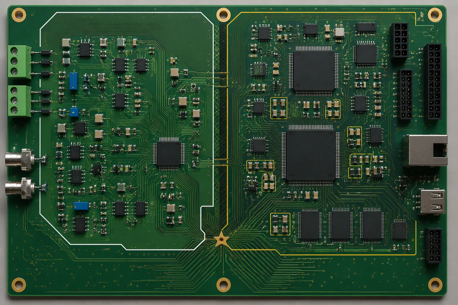
A single industrial automation pcb carries both delicate analog front end traces and fast digital buses. Layout decides whether those domains coexist or fight. Good sensor interface design starts with placement.
Analog And Digital Partitioning
Split the board into distinct functional zones. Keep sensors and amplifiers physically distant from CPUs and FPGAs. Place sensitive analog parts, such as amplifiers and voltage references, inside the analog plane. Put noisy digital parts, such as logic control and timing blocks, in the digital plane. A mixed-signal ADC with low digital current behaves like an analog component, so locate it in the analog plane. With multiple high-current converters, tie AVCC to analog and DVDD to digital. Even a universal interface needs clean zoning.
نظر | المجال التناظري | المجال الرقمي |
|---|---|---|
وضع المكون | Sensitive parts inside the analog plane | Noisy logic and timing blocks in the digital plane |
مزود الطاقة | Dedicated analog supply block, close to powered parts | Dedicated digital supply block |
أساس | Solid ground plane for low digital current; star-ground junction for complex high-current systems | نفسه |
Control grounding with one solid ground plane. Never let noisy digital return currents flow through the quiet analog ground area. Do not route digital traces across an analog section. If a crossing is unavoidable, route perpendicular to reduce interaction area. Place decoupling capacitors as close as possible to digital IC power pins. Avoid outdated split ground planes, which disrupt return paths and create inductive loops. Never overlap an analog power plane with a digital ground plane, because that overlap forms a capacitor that injects digital noise into the analog supply. Control impedance on high-speed digital traces and current capacity on analog power rails. Flexible sensor interfaces help when complex geometries or dynamic environments force the board into an unusual shape.
Routing, Shielding, And Thermal Design
Route critical analog sensor traces as differential pairs with adjacent ground or guard traces. This preserves signal fidelity against motor and drive EMI. Use smooth, curved traces instead of sharp corners to spread mechanical strain and prevent cracking. Keep trace widths uniform to avoid impedance disruptions. In high-density designs, stagger vias and traces across layers to remove weak points. For high-speed signals, control impedance through wider trace spacing or careful reference-plane use. Prefer cross-hatched planes over solid copper planes when you need flexibility plus shielding and return paths. Provide extra trace clearance near rigid-to-flex transitions, a common stress zone. For high-current paths, use wider or parallel traces plus stiffeners to cut resistance and heat buildup. This mixed-signal discipline يؤتي ثماره.
منطقة التصميم | تقنية | الهدف |
|---|---|---|
ملابس حرارية | Filled or staggered thermal vias beneath amplifiers and ADCs | Lowers thermal resistance |
ملابس حرارية | Copper pours as heat spreaders | Channels heat away from sensitive analog sections |
ملابس حرارية | Keep about 1.6 mm board thickness as an industrial baseline; simulate junction temperatures with FEA | Predicts hotspots |
التدريع | Solid ground planes with stitching vias along trace edges | Maintains low-impedance return paths |
تصميم | Centralize high-vibration parts near mounting points; use 45° bends | Shortens stress paths |
These practices keep your signal conditioning circuits quiet and your analog and digital sensors reliable. They protect the single data acquisition pcb through vibration and heat. They also give sensor fusion a clean foundation later, and they keep the data acquisition pcb ready for control.
الاختبار والتحقق من الصحة
Bench Characterization And Calibration
You test the board on the bench before it ever meets a real machine. Feed each channel a known reference and sweep it across the full input range. Record the output at every step. Compare the result to the ideal line and note the error. This sweep exposes gain errors, offset errors, and dead zones in your signal conditioning circuits. A channel that looks fine at mid-scale can drift badly near the rails.
Calibration turns those measurements into correction data. Store gain and offset coefficients in firmware for each channel. Apply them at runtime, so the raw reading becomes a corrected value. Repeat the calibration after a warm-up period, because thermal drift shifts the response. Check the noise floor too. Digital switching noise can peak at 100 mV, and analog thresholds can sit as low as 10 mV, so measure with the digital section running. A quiet board at power-off proves little.
EMI/EMC And Environmental Testing
Bench results mean nothing if the board fails in the field. Run radiated and conducted emissions tests in an accredited chamber. Apply immunity tests next: electrostatic discharge, burst, surge, and radio-frequency fields. Watch for upset in the analog front end during each test. A mixed-signal board often passes emissions and still fails immunity, because a transient couples into a sensitive input.
Then move to environmental testing. Cycle the board through its rated temperature range and log drift on every channel. Add vibration and humidity exposure for industrial duty. Verify that analog and digital sensors still read correctly after each stress. Run a long soak test to catch intermittent faults. Document every failure and its conditions. This record guides your next layout revision and gives you evidence for certification. Treat validation as part of sensor interface design, not an afterthought. It also builds the trusted data that sensor fusion depends on later.
التحديات الشائعة وحلولها
Crosstalk, Ground Loops, And Drift
Crosstalk, ground loops, and drift are the three faults that quietly ruin a mixed-signal board. Each one has a distinct cause, so each needs a distinct fix. استخدم الجدول أدناه to match the symptom to the remedy.
القضية | سبب | تخفيف |
|---|---|---|
حلقة أرضية | Multiple ground paths create circulating currents | Break the loop with a single-point star ground |
انجراف | Cable resistance shifts with temperature | Apply temperature compensation and recalibrate periodically |
إضعاف الإشارة | Long cable runs weaken the signal | Shorten runs or add amplification |
EMI | Motors, welders, and power distribution | Shield cables and reroute them away from noise |
عدم تطابق المعاوقة | Cable does not match the sensor or receiver | Match impedance at each connection point |
You can also cut crosstalk at the sensing layer. Common grounded electrodes, isolated sensing units, and a micropore isolation layer all help. So do microcage structures, serpentine interconnects, and trapezoidal prism designs. An embedded electrode layer with a common ground works well, and modular readout protocols keep large arrays scalable. Apply these ideas early in your sensor interface design, because retrofitting them later costs far more.
Diagnosing Intermittent Faults
Intermittent faults hide between good readings, so you need a method that catches them in time. A proven approach injects known faults and watches how the system responds. An incipient fault went into the iα current sensor at ر = 1.25 ثانية. An intermittent fault hit the ωe speed sensor from t = 0.5 s to 0.8 s, then again from t = 1.5 s to 1.8 s. A high-order sliding mode observer generated residuals for both sensors. An AcI-based index then processed those residuals. The result: the index missed the incipient current fault but caught both intermittent speed faults, with a delay.
Index-based methods give you a practical toolkit. MRI, MAI, MVI, MEI, DBI1, and DBI2 each compare a computed value against a threshold, and Otsu-based thresholding sets that threshold. You build the indices from fused speed, current, and voltage residuals. This approach relies on one sensor per channel, and a fault in one channel affects the others, so the indices separate faulty channels from healthy ones. That separation supports sensor fusion later, because you know which channels to trust. Keep your signal conditioning circuits and data acquisition pcb clean, and these diagnostics will find the faults that analog and digital sensors alone cannot reveal.
Edge Processing And Sensor Fusion
On-Board Data Fusion
You can move the first layer of sensor fusion onto the board itself. A local controller combines readings from multiple sensors before any data leaves the node. This step cuts bus traffic and shortens the path to a control decision. Your mixed-signal front end already digitizes each channel, so the processor sees clean numbers instead of raw voltages.
Timing sets the limit here. Wired paths respond in about 20–60 µs, with a worst case near 100 µs. Wireless links run slower: WISA and WSAN-FA target about 10 ms, and IO-Link Wireless targets about 5 ms. Keep your sensor fusion math inside that budget. A fusion routine that takes longer than the loop period defeats the purpose. Start with simple weighted averages, then add complexity only when the timing allows.
Future Interface Trends
Expect tighter integration in the years ahead. Multi-channel front-end ICs will absorb more of the work now done by discrete signal conditioning circuits. Digital sensor buses will simplify wiring for analog and digital sensors on one platform. Reconfigurable sensor interfaces will let one board serve many product lines without a layout change. These trends reward designers who plan headroom now.
Edge processing will also grow smarter. Local sensor fusion will handle fault detection, drift correction, and data reduction before transmission. That shift matters for multi-sensor interfaces in large installations, where bandwidth and power are scarce. Build your next board with spare compute and a clean partition between domains. You will thank yourself when the firmware grows.
Start with each sensor’s signal characteristics. Condition and isolate early. Choose mixed-signal ICs wisely, because programmable analog blocks let you change the signal path in software instead of respinning the board. Partition your single industrial automation pcb with care. Then validate against real industrial conditions.
Keep these takeaways close:
Shield cables, ground properly, and use differential signaling such as RS-485 for long runs.
Use smart pin multiplexing, RTOS scheduling, and DMA for smooth multi-protocol operation.
Debug with logic analyzers and document pin assignments.
Expect tighter integration ahead: multi-channel front-end ICs, digital sensor buses, reconfigurable interfaces, and edge sensor fusion. Build a small prototype first. Test it early in industrial automation, and let each result guide the next revision.
الأسئلة الشائعة
How do I pick between a wired and a wireless sensor interface?
Start with your loop timing. A wired path responds in about 20–60 µs, with a worst case near 100 µs. Wireless links run slower: WISA and WSAN-FA target about 10 ms, and IO-Link Wireless targets about 5 ms. Choose wireless only when the loop budget allows it.
How much board space can a mixed-signal interface IC save me?
You can save up to 90% of board area versus a discrete solution. The IC replaces separate op-amps, comparators, references, and passives with configurable on-chip blocks. You also change behavior in software instead of respinning the layout.
What ADC resolution do I need for my sensors?
Match resolution to the job. General monitoring works well at 10–12 bits. Precision work needs 16–24 bits. An MCU’s built-in ADC usually tops out at 12 bits, so go external for higher resolution, simultaneous sampling, or input isolation.
Why does my analog channel read fine on the bench but fail in the field?
Bench tests often run with the digital section quiet. Digital switching noise can peak at 100 mV, and analog thresholds can sit as low as 10 mV. Measure with the digital section running, then confirm with immunity tests such as ESD, burst, and surge.
Should I split my ground plane between analog and digital?
No. Use one solid ground plane and keep noisy digital return currents out of the quiet analog area. Splits disrupt return paths and distort high-frequency signals. Connect analog and digital grounds at a single point near the power supply entry instead.